ZHCSCW5B August   2014  – September 2017 LM43600

PRODUCTION DATA.  

  1. 特性
  2. 应用
  3. 说明
  4. 简化电路原理图
    1.     5
    2.     辐射发射图VIN = 12V,VOUT = 3.3V,FSW= 500kHz,IOUT = 0.5A
  5. 修订历史记录
  6. Pin Configuration and Functions
    1.     Pin Functions
  7. Specifications
    1. 7.1 Absolute Maximum Ratings
    2. 7.2 ESD Ratings
    3. 7.3 Recommended Operating Conditions
    4. 7.4 Thermal Information
    5. 7.5 Electrical Characteristics
    6. 7.6 Timing Requirements
    7. 7.7 Switching Characteristics
    8. 7.8 Typical Characteristics
  8. Detailed Description
    1. 8.1 Overview
    2. 8.2 Functional Block Diagram
    3. 8.3 Feature Description
      1. 8.3.1  Fixed Frequency Peak Current Mode Controlled Step-Down Regulator
      2. 8.3.2  Light Load Operation
      3. 8.3.3  Adjustable Output Voltage
      4. 8.3.4  Enable (ENABLE)
      5. 8.3.5  VCC, UVLO and BIAS
      6. 8.3.6  Soft Start and Voltage Tracking (SS/TRK)
      7. 8.3.7  Switching Frequency (RT) and Synchronization (SYNC)
      8. 8.3.8  Minimum ON-Time, Minimum OFF-Time and Frequency Foldback at Dropout Conditions
      9. 8.3.9  Internal Compensation and CFF
      10. 8.3.10 Bootstrap Voltage (BOOT)
      11. 8.3.11 Power Good (PGOOD)
      12. 8.3.12 Overcurrent and Short-Circuit Protection
      13. 8.3.13 Thermal Shutdown
    4. 8.4 Device Functional Modes
      1. 8.4.1 Shutdown Mode
      2. 8.4.2 Stand-by Mode
      3. 8.4.3 Active Mode
      4. 8.4.4 CCM Mode
      5. 8.4.5 Light Load Operation
      6. 8.4.6 Self-Bias Mode
  9. Applications and Implementation
    1. 9.1 Application Information
    2. 9.2 Typical Applications
      1. 9.2.1 Design Requirements
      2. 9.2.2 Detailed Design Procedure
        1. 9.2.2.1  Custom Design With WEBENCH® Tools
        2. 9.2.2.2  Output Voltage Setpoint
        3. 9.2.2.3  Switching Frequency
        4. 9.2.2.4  Input Capacitors
        5. 9.2.2.5  Inductor Selection
        6. 9.2.2.6  Output Capacitor Selection
        7. 9.2.2.7  Feedforward Capacitor
        8. 9.2.2.8  Bootstrap Capacitors
        9. 9.2.2.9  VCC Capacitor
        10. 9.2.2.10 BIAS Capacitors
        11. 9.2.2.11 Soft-Start Capacitors
        12. 9.2.2.12 Undervoltage Lockout Setpoint
        13. 9.2.2.13 PGOOD
      3. 9.2.3 Application Performance Curves
  10. 10Power Supply Recommendations
  11. 11Layout
    1. 11.1 Layout Guidelines
      1. 11.1.1 Compact Layout for EMI Reduction
      2. 11.1.2 Ground Plane and Thermal Considerations
      3. 11.1.3 Feedback Resistors
    2. 11.2 Layout Example
  12. 12器件和文档支持
    1. 12.1 开发支持
      1. 12.1.1 使用 WEBENCH® 工具创建定制设计
    2. 12.2 接收文档更新通知
    3. 12.3 社区资源
    4. 12.4 商标
    5. 12.5 静电放电警告
    6. 12.6 Glossary
  13. 13机械、封装和可订购信息

封装选项

请参考 PDF 数据表获取器件具体的封装图。

机械数据 (封装 | 引脚)
  • PWP|16
散热焊盘机械数据 (封装 | 引脚)
订购信息

Application Performance Curves

See Table 2 for bill of materials for each VOUT and FS combination. Unless otherwise stated, application performance curves were taken at TA = 25 °C.
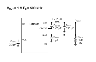
LM43600 Sch_BOM_1V500k.gif
VIN = 12 V
Figure 47. BOM for VOUT = 1 V FS = 500 kHz
LM43600 C011_Reg_43600_1V500k.png
VOUT = 1 V FS = 500 kHz
Figure 49. Output Voltage Regulation
LM43600 12VIN_1VO_500k_50mATO500mA.gif
VOUT = 1 V FS = 500 kHz VIN = 12 V
Figure 51. Load Transient Between 0.05 A and 0.5 A
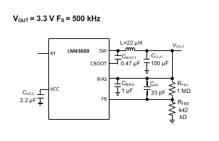
LM43600 Sch_BOM_3.3V500k.gif
VIN = 12 V
Figure 53. BOM for VOUT = 3.3 V FS = 500 kHz
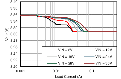
LM43600 C012_Reg_43600_3p3V500k.png
VOUT = 3.3 V FS = 500 kHz
Figure 55. Output Voltage Regulation
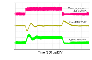
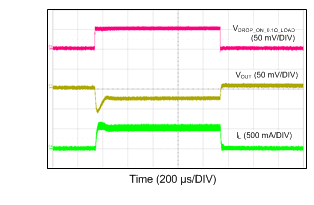
LM43600 12VIN_3p3VO_500k_50mATO500mA.gif
VOUT = 3.3 V FS = 500 kHz VIN = 12 V
Figure 57. Load Transient Between 0.05 A and 0.5 A
LM43600 Sch_BOM_5V500k.gif
VIN = 12 V
Figure 59. BOM for VOUT = 5 V, FS = 500 kHz
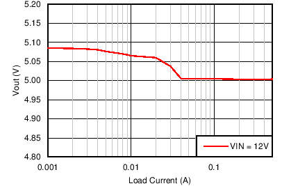
LM43600 C013_Reg_43600_5V500k.png
VOUT = 5 V FS = 500 kHz
Figure 61. Output Voltage Regulation
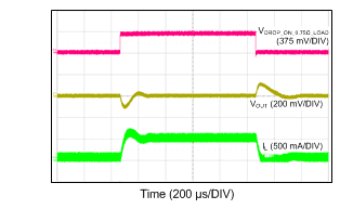
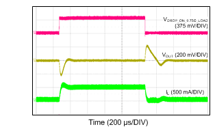
LM43600 12VIN_5VO_500k_50mATO500mA.gif
VOUT = 5 V FS = 500 kHz VIN = 12 V
Figure 63. Load Transient Between 0.05 A and 0.5 A
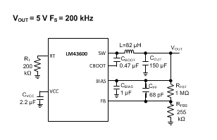
LM43600 Sch_BOM_5V200k.gif
VIN = 12 V
Figure 65. BOM for VOUT = 5 V, FS = 200 kHz
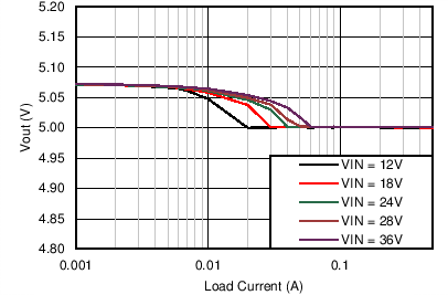
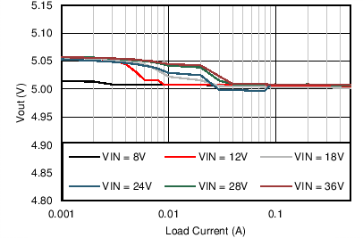
LM43600 C014_Reg_43600_5V200k.png
VOUT = 5 V FS = 200 kHz
Figure 67. Output Voltage Regulation
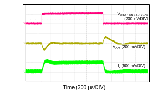
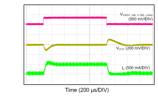
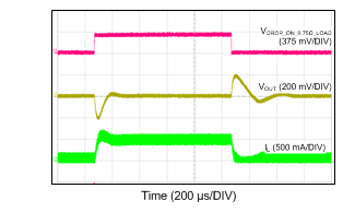
LM43600 12VIN_5VO_200k_50mATO500mA.gif
VOUT = 5 V FS = 200 kHz VIN = 12 V
Figure 69. Load Transient Between 0.05 A and 0.5 A
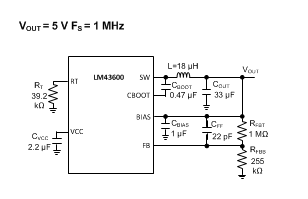
LM43600 Sch_BOM_5V1M.gif
VIN = 12 V
Figure 71. BOM for VOUT = 5 V FS = 1 MHz
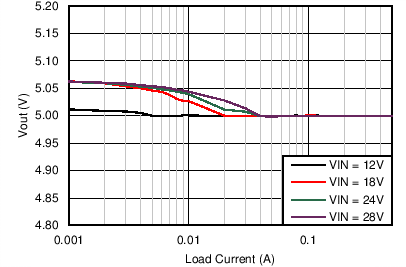
LM43600 C015_Reg_43600_5V1M.png
VOUT = 5 V FS = 1 MHz
Figure 73. Output Voltage Regulation
LM43600 12VIN_5VO_1M_50mATO500mA.gif
VOUT = 5 V FS = 1 MHz VIN = 12 V
Figure 75. Load Transient Between 0.05 A and 0.5 A
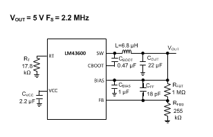
LM43600 Sch_BOM_5V2p2M.gif
VIN = 12 V
Figure 77. BOM for VOUT = 5 V, FS = 2.2 MHz
LM43600 C016_Reg_43600_5V2p2M.png
VOUT = 5 V FS = 2.2 MHz
Figure 79. Output Voltage Regulation
LM43600 12VIN_5VO_2p2M_50mATO500mA.gif
VOUT = 5 V FS = 2.2 MHz VIN = 12 V
Figure 81. Load Transient Between 0.05 A and 0.5 A
LM43600 Sch_BOM_12V500k.gif
VIN = 24 V
Figure 83. BOM for VOUT = 12 V, FS = 500 kHz
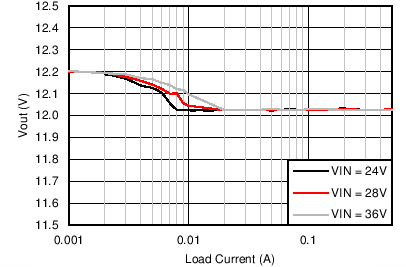
LM43600 C017_Reg_43600_12V500k.png
VOUT = 12 V FS = 500 kHz
Figure 85. Output Voltage Regulation
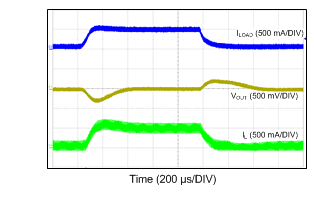
LM43600 24VIN_12VO_500k_50mATO500mA.gif
VOUT = 12 V FS = 500 kHz VIN = 24 V
Figure 87. Load Transient Between 0.05 A and 0.5 A
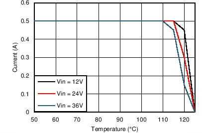
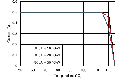
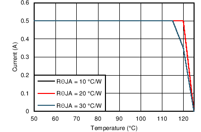
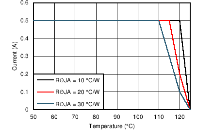
LM43600 3p3VO_500kThetaJA20CpW.png
VOUT = 3.3 V FS = 500 kHz
Figure 89. Derating Curve with RθJA = 20°C/W
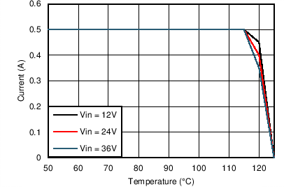
LM43600 5VO_200kThetaJA20CpW.png
VOUT = 5 V FS = 200 kHz
Figure 91. Derating Curve with RθJA = 20°C/W
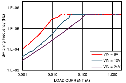
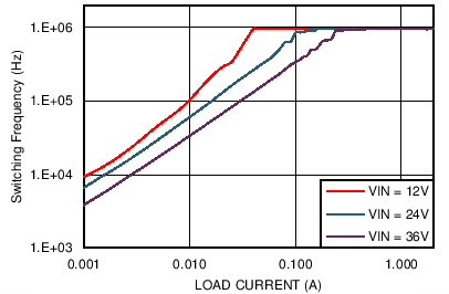
LM43600 3p3V_500k_Fsw_PFM.png
VOUT = 3.3 V FS = 500 kHz
Figure 93. Switching Frequency vs IOUT in PFM Operation
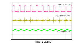
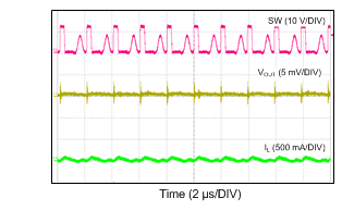
LM43600 12VIN_3V3_500k_500mA_CCM.gif
VOUT = 3.3 V FS = 500 kHz IOUT = 0.5 A
Figure 95. Switching Waveform in CCM Operation
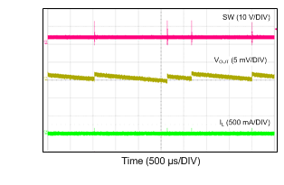
LM43600 12VIN_3V3_500k_0mA_PFM.gif
VOUT = 3.3 V FS = 500 kHz IOUT = 0 mA
Figure 97. Switching Waveform in PFM Operation
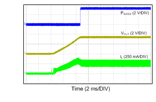
LM43600 12VIN_3p3VO_500k_250mA.gif
VIN = 12 V VOUT = 3.3 V RLOAD = 13.2 Ω
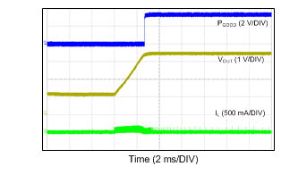
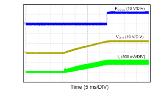
Figure 99. Start-up Into Half Load with Internal Soft-Start Rate
LM43600 12VIN_3p3VO_500k_PREBIAS_1V.gif
VIN = 12 V VOUT = 3.3 V RLOAD = Open
Figure 101. Start-up Into 1-V Pre-biased Voltage
LM43600 12TO36V_3V3_500k_250mA_1V1us.gif
VOUT = 3.3 V FS = 500 kHz IOUT = 0.25 A
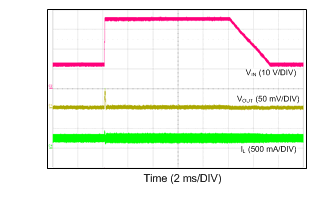
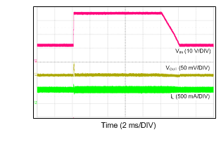
Figure 103. Line Transient: VIN Transitions Between 12 V and 36 V
LM43600 12VIN_3p3VO_500k_500mA_SHORT_RECOVERY.gif
VOUT = 3.3 V FS = 500 kHz VIN = 12 V
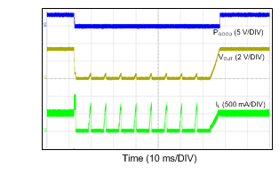
Figure 105. Short-Circuit Protection and Recover
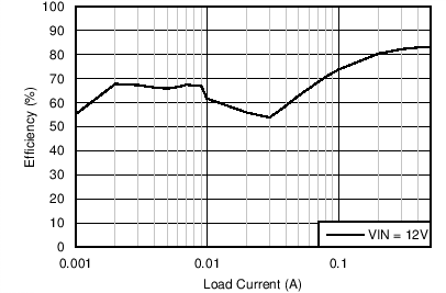
LM43600 C001_Eff_43600_1V500k.png
VOUT = 1 V FS = 500 kHz
Figure 48. Efficiency
LM43600 12VIN_1VO_500k_0mATO500mA.gif
VOUT = 1 V FS = 500 kHz VIN = 12 V
Figure 50. Load Transient Between 0 A and 0.5 A
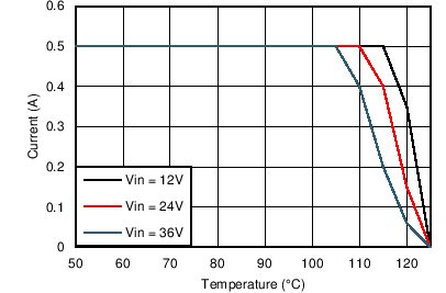
LM43600 12V_1VO_500kThetaJA.png
VOUT = 1 V FS = 500 kHz VIN = 12 V
Figure 52. Derating Curve
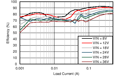
LM43600 C002_Eff_43600_3p3V500k.png
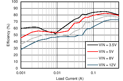
VOUT = 3.3 V FS = 500 kHz
Figure 54. Efficiency
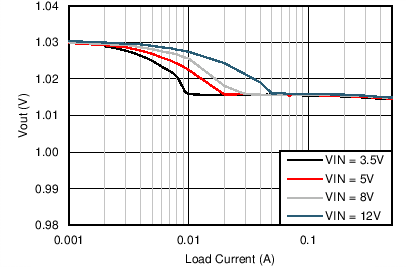
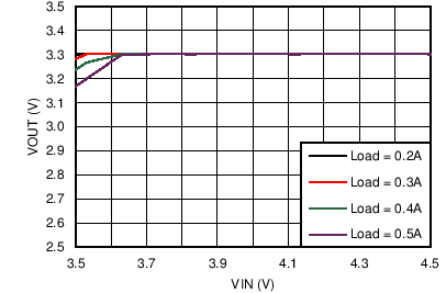
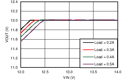
LM43600 C022_DO_43600_3p3V500k.png
VOUT = 3.3 V FS = 500 kHz
Figure 56. Dropout Curve
LM43600 12V_3p3VO_500kThetaJA.png
VOUT = 3.3 V FS = 500 kHz VIN = 12 V
Figure 58. Derating Curve
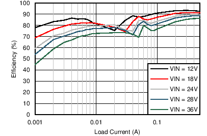
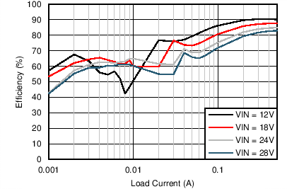
LM43600 C003_Eff_43600_5V500k.png
VOUT = 5 V FS = 500 kHz
Figure 60. Efficiency
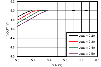
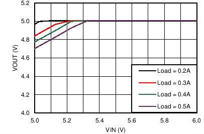
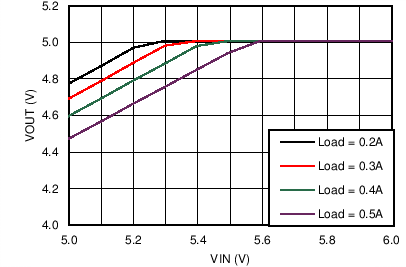
LM43600 C023_DO_43600_5V500k.png
VOUT = 5 V FS = 500 kHz
Figure 62. Dropout Curve
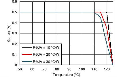
LM43600 12V_5VO_500kThetaJA.png
VOUT = 5 V FS = 500 kHz VIN = 12 V
Figure 64. Derating Curve
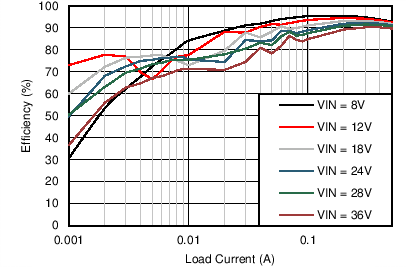
LM43600 C004_Eff_43600_5V200k.png
VOUT = 5 V FS = 200 kHz
Figure 66. Efficiency
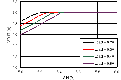
LM43600 C024_DO_43600_5V200k.png
VOUT = 5 V FS = 200 kHz
Figure 68. Dropout Curve
LM43600 12V_5VO_200kThetaJA.png
VOUT = 5 V FS = 200 kHz VIN = 12 V
Figure 70. Derating Curve
LM43600 C005_Eff_43600_5V1M.png
VOUT = 5 V FS = 1 MHz VIN = 12 V
Figure 72. Efficiency
LM43600 C025_DO_43600_5V1M.png
VOUT = 5 V FS = 1 MHz
Figure 74. Dropout Curve
LM43600 12V_5VO_1000kThetaJA.png
VOUT = 5 V FS = 1 MHz VIN = 12 V
Figure 76. Derating Curve
LM43600 C006_Eff_43600_5V2p2M.png
VOUT = 5 V FS = 2.2 MHz VIN = 12 V
Figure 78. Efficiency
LM43600 C026_DO_43600_5V2p2M.png
VOUT = 5 V FS = 2.2 MHz
Figure 80. Dropout Curve
LM43600 12V_5VO_2200kThetaJA.png
VOUT = 5 V FS = 2.2 MHz VIN = 12 V
Figure 82. Derating Curve
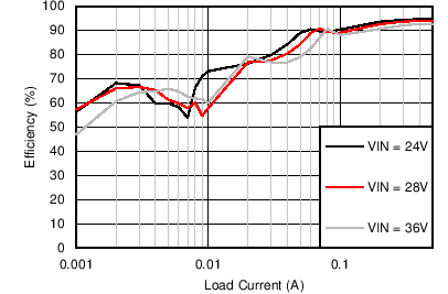
LM43600 C007_Eff_43600_12V500k.png
VOUT = 12 V FS = 500 kHz
Figure 84. Efficiency
LM43600 C027_DO_43600_12V500k.png
VOUT = 12 V FS = 500 kHz
Figure 86. Dropout Curve
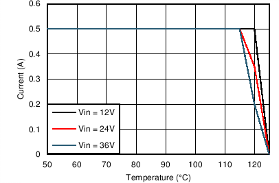
LM43600 24V_12VO_500kThetaJA.png
VOUT = 12 V FS = 500 kHz VIN = 24 V
Figure 88. Derating Curve
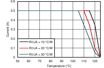
LM43600 5VO_500kThetaJA20CpW.png
VOUT = 5 V FS = 500 kHz
Figure 90. Derating Curve with RθJA = 20°C/W
LM43600 5VO_1000kThetaJA20CpW.png
VOUT = 5 V FS = 1 MHz
Figure 92. Derating Curve with RθJA = 20°C/W
LM43600 5V_1M_Fsw_PFM.png
VOUT = 5 V FS = 1 MHz
Figure 94. Switching Frequency vs IOUT in PFM Operation
LM43600 12VIN_3V3_500k_10mA_DCM.gif
VOUT = 3.3 V FS = 500 kHz IOUT =10 mA
Figure 96. Switching Waveform in DCM Operation
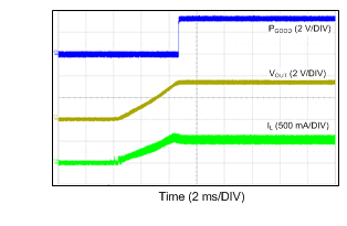
LM43600 12VIN_3p3VO_500k_500mA.gif
VIN = 12 V VOUT = 3.3 V RLOAD = 6.6 Ω
Figure 98. Start-up Into Full Load with Internal Soft-Start Rate
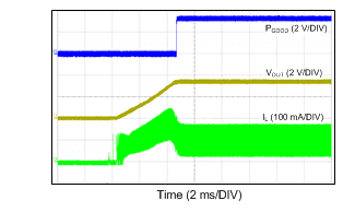
LM43600 12VIN_3p3VO_500k_100mA.gif
VIN = 12 V VOUT = 3.3 V RLOAD = 33 Ω
Figure 100. Start-up Into 100 mA with Internal Soft-Start Rate
LM43600 24VIN_12VO_500k_500mA_33nFCss.gif
VIN = 24 V VOUT = 12 V RLOAD = 6 Ω
Figure 102. Start-up with External Capacitor CSS
LM43600 12TO36V_3V3_500k_500mA_1V1us.gif
VOUT = 3.3 V FS = 500 kHz IOUT = 0.5 A
Figure 104. Line Transient: VIN Transitions Between 12 V and 36 V