ZHCSCW5B August 2014 – September 2017 LM43600
PRODUCTION DATA.
- 1 特性
- 2 应用
- 3 说明
- 4 简化电路原理图
- 5 修订历史记录
- 6 Pin Configuration and Functions
- 7 Specifications
-
8 Detailed Description
- 8.1 Overview
- 8.2 Functional Block Diagram
- 8.3
Feature Description
- 8.3.1 Fixed Frequency Peak Current Mode Controlled Step-Down Regulator
- 8.3.2 Light Load Operation
- 8.3.3 Adjustable Output Voltage
- 8.3.4 Enable (ENABLE)
- 8.3.5 VCC, UVLO and BIAS
- 8.3.6 Soft Start and Voltage Tracking (SS/TRK)
- 8.3.7 Switching Frequency (RT) and Synchronization (SYNC)
- 8.3.8 Minimum ON-Time, Minimum OFF-Time and Frequency Foldback at Dropout Conditions
- 8.3.9 Internal Compensation and CFF
- 8.3.10 Bootstrap Voltage (BOOT)
- 8.3.11 Power Good (PGOOD)
- 8.3.12 Overcurrent and Short-Circuit Protection
- 8.3.13 Thermal Shutdown
- 8.4 Device Functional Modes
-
9 Applications and Implementation
- 9.1 Application Information
- 9.2
Typical Applications
- 9.2.1 Design Requirements
- 9.2.2
Detailed Design Procedure
- 9.2.2.1 Custom Design With WEBENCH® Tools
- 9.2.2.2 Output Voltage Setpoint
- 9.2.2.3 Switching Frequency
- 9.2.2.4 Input Capacitors
- 9.2.2.5 Inductor Selection
- 9.2.2.6 Output Capacitor Selection
- 9.2.2.7 Feedforward Capacitor
- 9.2.2.8 Bootstrap Capacitors
- 9.2.2.9 VCC Capacitor
- 9.2.2.10 BIAS Capacitors
- 9.2.2.11 Soft-Start Capacitors
- 9.2.2.12 Undervoltage Lockout Setpoint
- 9.2.2.13 PGOOD
- 9.2.3 Application Performance Curves
- 10Power Supply Recommendations
- 11Layout
- 12器件和文档支持
- 13机械、封装和可订购信息
8.3.7 Switching Frequency (RT) and Synchronization (SYNC)
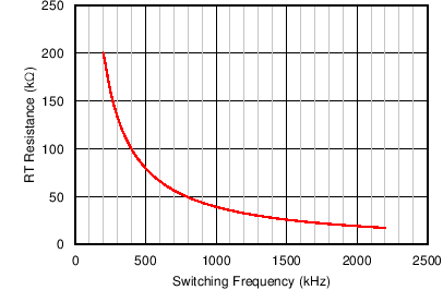
The switching frequency of the LM43600 can be programmed by the impedance RT from the RT pin to ground. The frequency is inversely proportional to the RT resistance. The RT pin can be left floating and the LM43600 will operate at 500 kHz default switching frequency. The RT pin is not designed to be shorted to ground.
For a desired frequency, typical RT resistance can be found by Equation 3.
Figure 40 shows RT resistance vs switching frequency FS curve.
 Figure 40. RT Resistance vs Switching Frequency
Table 1 provides typical RT values for a given FS.
Table 1. Typical Frequency Setting RT Resistance
| FS (kHz) | RT (kΩ) |
|---|---|
| 200 | 200 |
| 350 | 115 |
| 500 | 80.6 |
| 750 | 53.6 |
| 1000 | 39.2 |
| 1500 | 26.1 |
| 2000 | 19.6 |
| 2200 | 17.8 |
The LM43600 switching action can also be synchronized to an external clock from 200 kHz to 2.2 MHz. Connect an external clock to the SYNC pin, with proper high speed termination, to avoid ringing. The SYNC pin should be grounded if not used.
 Figure 41. Frequency Synchronization
The recommendations for the external clock include high level no lower than 2 V, low level no higher than 0.4 V, duty cycle between 10% and 90% and both positive and negative pulse width no shorter than 80 ns. When the external clock fails at logic high or low, the LM43600 will switch at the frequency programmed by the RT resistor after a time-out period. It is recommended to connect a resistor RT to the RT pin such that the internal oscillator frequency is the same as the target clock frequency when the LM43600 is synchronized to an external clock. This allows the regulator to continue operating at approximately the same switching frequency if the external clock fails.
The choice of switching frequency is usually a compromise between conversion efficiency and the size of the circuit. Lower switching frequency implies reduced switching losses (including gate charge losses, switch transition losses, etc.) and usually results in higher overall efficiency. However, higher switching frequency allows use of smaller LC output filters and hence a more compact design. Lower inductance also helps transient response (higher large signal slew rate of inductor current), and reduces the DCR loss. The optimal switching frequency is usually a trade-off in a given application and thus needs to be determined on a case-by-case basis. It is related to the input voltage, output voltage, most frequent load current level(s), external component choices, and circuit size requirement. The choice of switching frequency may also be limited if an operating condition triggers TON-MIN or TOFF-MIN.