ZHCSDN2 April 2015 LM3632A
PRODUCTION DATA.
- 1 特性
- 2 应用
- 3 说明
- 4 修订历史记录
- 5 Pin Configuration and Functions
- 6 Specifications
-
7 Detailed Description
- 7.1 Overview
- 7.2 Functional Block Diagram
- 7.3
Features Description
- 7.3.1 Backlight
- 7.3.2 LCM Bias
- 7.3.3 Flash
- 7.3.4 Software RESET
- 7.3.5 EN Input
- 7.3.6 Thermal Shutdown (TSD)
- 7.4 Device Functional Modes
- 7.5 Programming
- 7.6
Register Maps
- 7.6.1 Revision (Address = 0x01) [reset = 0x05]
- 7.6.2 Backlight Configuration1 (Address = 0x02) [reset = 0x30]
- 7.6.3 Backlight Configuration2 (Address = 0x03) [reset = 0x0D]
- 7.6.4 Backlight Brightness LSB (Address = 0x04) [reset = 0x07]
- 7.6.5 Backlight Brightness MSB (Address = 0x05) [reset = 0xFF]
- 7.6.6 Flash/Torch Current (Address = 0x06) [reset = 0x3E]
- 7.6.7 Flash Configuration (Address = 0x07) [reset = 0x2F]
- 7.6.8 VIN Monitor (Address = 0x08) [reset = 0x03]
- 7.6.9 I/O Control (Address = 0x09) [reset = 0x00]
- 7.6.10 Enable (Address = 0x0A) [reset = 0x00]
- 7.6.11 Flags1 (Address = 0x0B) [reset = 0x00]
- 7.6.12 Display Bias Configuration (Address = 0x0C) [reset = 0x18]
- 7.6.13 LCM Boost Bias (Address = 0x0D) [reset = 0x1E]
- 7.6.14 VPOS Bias (Address = 0x0E) [reset = 0x1E]
- 7.6.15 VNEG Bias (Address = 0x0F) [reset = 0x1C]
- 7.6.16 Flags2 (Address = 0x10) [reset = 0x00]
- 8 Application and Implementation
- 9 Power Supply Recommendations
- 10Layout
- 11器件和文档支持
- 12机械、封装和可订购信息
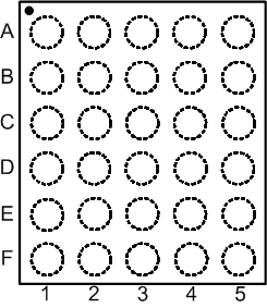
5 Pin Configuration and Functions
YFF Package
30-Pin DSBGA
Top View

Pin Functions
| PIN | TYPE | DESCRIPTION | |
|---|---|---|---|
| NUMBER | NAME | ||
| A1 | VPOS | O | Positive LDO output for LCM bias power |
| A2 | LCM_OUT | O | LCM bias boost output voltage |
| A3 | LCM_SW | O | LCM bias boost switch connection |
| A4 | BL_GND | - | Backlight boost ground connection |
| A5 | BL_SW | O | Backlight boost switch connection |
| B1 | LCM_EN2 | I | Enable for inverting charge pump output |
| B2 | LCM_EN1 | I | Enable for positive LDO output |
| B3 | EN | I | Active high chip enable |
| B4 | LCM_GND | - | LCM bias boost ground connection |
| B5 | BL_OUT | O | Backlight boost output voltage |
| C1 | C1 | O | Inverting charge pump flying capacitor positive connection |
| C2 | SDA | I/O | Serial data connection for I2C- compatible interface |
| C3 | TX | I | Flash interrupt input |
| C4 | AGND | - | Analog ground connection |
| C5 | BLED1 | O | Input pin to internal LED current sink 1 |
| D1 | CP_GND | - | Inverting charge pump ground connection |
| D2 | SCL | I | Serial clock connection for I2C- compatible interface |
| D3 | STROBE | I | Flash enable input |
| D4 | PWM | I | PWM input for CABC current control |
| D5 | BLED2 | O | Input pin to internal LED current sink 2 |
| E1 | C2 | O | Inverting charge pump flying capacitor negative connection |
| E2 | FLED | O | High-side current source output for flash LED |
| E3 | FL_OUT | O | Flash boost output voltage |
| E4 | FL_SW | O | Flash boost switch connection |
| E5 | VIN | I | Input voltage connection |
| F1 | VNEG | O | Inverting charge pump output voltage |
| F2 | FLED | O | High-side current source output for flash LED |
| F3 | FL_OUT | O | Flash boost output voltage |
| F4 | FL_SW | O | Flash boost switch connection |
| F5 | FL_GND | - | Flash boost ground connection |