SNVS178H January 2002 – December 2015 LM3485
PRODUCTION DATA.
- 1 Features
- 2 Applications
- 3 Description
- 4 Revision History
- 5 Pin Configuration and Functions
- 6 Specifications
- 7 Detailed Description
-
8 Application and Implementation
- 8.1 Application Information
- 8.2
Typical Application
- 8.2.1 Design Requirements
- 8.2.2
Detailed Design Procedure
- 8.2.2.1 Step by Step Design Procedure
- 8.2.2.2 Inductor Selection (L1)
- 8.2.2.3 Output Voltage Set Point
- 8.2.2.4 Output Capacitor Selection (COUT)
- 8.2.2.5 Input Capacitor Selection (CIN)
- 8.2.2.6 Programming the Current Limit (RADJ)
- 8.2.2.7 Catch Diode Selection (D1)
- 8.2.2.8 P-Channel MOSFET Selection (Q1)
- 8.2.3 Application Curves
- 9 Power Supply Recommendations
- 10Layout
- 11Device and Documentation Support
- 12Mechanical, Packaging, and Orderable Information
6 Specifications
6.1 Absolute Maximum Ratings
over operating free-air temperature range (unless otherwise noted)(1)| MIN | TYP | MAX | UNIT | ||
|---|---|---|---|---|---|
| PGATE voltage | −0.3 | 36 | V | ||
| FB voltage | −0.3 | 5 | V | ||
| ISENSE voltage | −1.0 | 36 | V | ||
| ADJ voltage | −0.3 | 36 | V | ||
| Maximum junction temperature | 150 | °C | |||
| Power dissipation (at TA = 25°C) | 417 | mW | |||
| Lead temperature | Vapor phase (60 sec.) | 215 | °C | ||
| Infrared (15 sec.) | 220 | °C | |||
| Storage temperature, Tstg | −65 | 160 | °C | ||
(1) Stresses beyond those listed under Absolute Maximum Ratings may cause permanent damage to the device. These are stress ratings only, which do not imply functional operation of the device at these or any other conditions beyond those indicated under Recommended Operating Conditions. Exposure to absolute-maximum-rated conditions for extended periods may affect device reliability.
6.2 ESD Ratings
| VALUE | UNIT | |||
|---|---|---|---|---|
| V(ESD) | Electrostatic discharge | Human-body model (HBM), per ANSI/ESDA/JEDEC JS-001(1) | ±2000 | V |
(1) JEDEC document JEP155 states that 500-V HBM allows safe manufacturing with a standard ESD control process.
6.3 Recommended Operating Conditions
| MIN | NOM | MAX | UNIT | ||
|---|---|---|---|---|---|
| Supply voltage | 4.5 | 35 | V | ||
| TJ | Operating junction temperature | −40 | 125 | °C | |
6.4 Thermal Information
| THERMAL METRIC(1) | LM3485 | UNIT | |
|---|---|---|---|
| DGK (VSSOP) | |||
| 8 PINS | |||
| RθJA | Junction-to-ambient thermal resistance | 163.3 | °C/W |
| RθJC(top) | Junction-to-case (top) thermal resistance | 56.7 | °C/W |
| RθJB | Junction-to-board thermal resistance | 83.2 | °C/W |
| ψJT | Junction-to-top characterization parameter | 5.9 | °C/W |
| ψJB | Junction-to-board characterization parameter | 81.9 | °C/W |
| RθJC(bot) | Junction-to-case (bottom) thermal resistance | N/A | °C/W |
(1) For more information about traditional and new thermal metrics, see the Semiconductor and IC Package Thermal Metrics application report, SPRA953.
6.5 Electrical Characteristics
Specifications are for TJ = 25°C. Unless otherwise specified, VIN = 12 V, VISNS = VIN − 1 V, and VADJ = VIN − 1.1 V. Data sheet minimum and maximum specification limits are specified by design, test, or statistical analysis.| PARAMETER | TEST CONDITIONS | MIN(1) | TYP(2) | MAX(1) | UNIT | ||
|---|---|---|---|---|---|---|---|
| IQ | Quiescent current at ground pin | FB = 1.5 V (Not Switching) | 250 | µA | |||
| (TJ = −40°C to 125°C) | 400 | ||||||
| VFB | Feedback voltage(3) | 1.226 | 1.242 | 1.258 | V | ||
| (TJ = −40°C to 125°C) | 1.217 | 1.267 | |||||
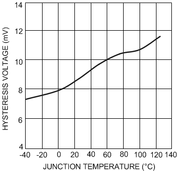
| VHYST | Comparator hysteresis | 10 | 15 | mV | |||
| (TJ = −40°C to 125°C) | 14 | 20 | |||||
| VCL(4) | Current limit comparator trip voltage | RADJ = 20 kΩ | 110 | mV | |||
| RADJ = 160 kΩ | 880 | ||||||
| VCL_OFFSET | Current limit comparator offset | VFB = 1.5 V | 0 | mV | |||
| (TJ = −40°C to 125°C) | −20 | 20 | |||||
| ICL_ADJ | Current limit ADJ current source | VFB = 1.5 V | 5.5 | µA | |||
| (TJ = −40°C to 125°C) | 3.0 | 7.0 | |||||
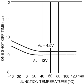
| TONMIN_CLCL | Current limit one shot off time | VADJ = 11.5 V VISNS = 11.0 V VFB = 1.0 V |
9 | µs | |||
| (TJ = −40°C to 125°C) | 6 | 14 | |||||
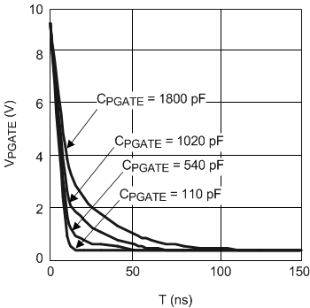
| RPGATE | Driver resistance | Source ISOURCE = 100 mA |
5.5 | Ω | |||
| Sink ISink = 100 mA |
8.5 | ||||||
| IPGATE | Driver output current | Source VIN = 7 V, PGATE = 3.5 V |
0.44 | A | |||
| Sink VIN = 7 V, PGATE = 3.5 V |
0.32 | ||||||
| IFB | FB pin bias current(5) | VFB = 1.0 V | 300 | nA | |||
| (TJ = −40°C to 125°C) | 750 | ||||||
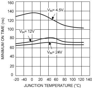
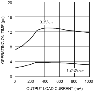
| TONMIN_NOR | Minimum on time in normal operation | VISNS = VADJ + 0.1 V Cload on OUT = 1000 pF(6) |
100 | ns | |||
| T | Minimum on time in current limit | VISNS = VADJ + 0.1 V VFB = 1.0 V Cload on OUT = 1000 pF(6) |
175 | ns | |||
| %VFB/ΔVIN | Feedback voltage line regulation | 4.5 ≤ VIN ≤ 35 V | 0.010% | ||||
(1) All limits are at room temperature unless otherwise specified. All room temperature limits are 100% tested. All limits at temperature extremes are specified via correlation using standard Statistical Quality Control (SQC) methods. All limits are used to calculate Average Outgoing Quality Level (AOQL).
(2) Typical numbers are at 25°C and represent the most likely norm.
(3) The VFB is the trip voltage at the FB pin when PGATE switches from high to low.
(4) VCL = ICL_ADJ × RADJ
(5) Bias current flows out from the FB pin.
(6) A 1000-pF capacitor is connected between VIN and PGATE.
6.6 Typical Characteristics
Unless otherwise specified, TJ = 25°C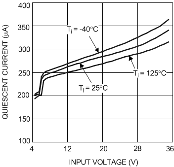
| FB = 1.5 V |
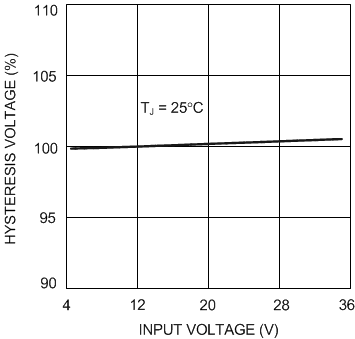
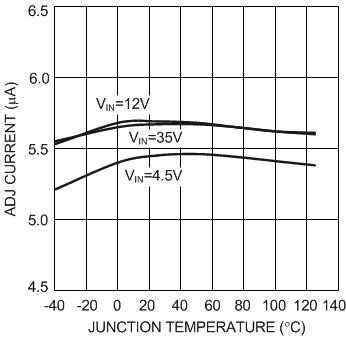
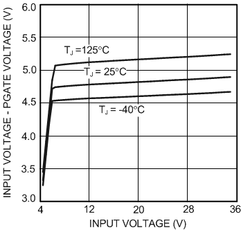
| VIN = 12 V |
| VOUT = 3.3 V | L = 22 µH |
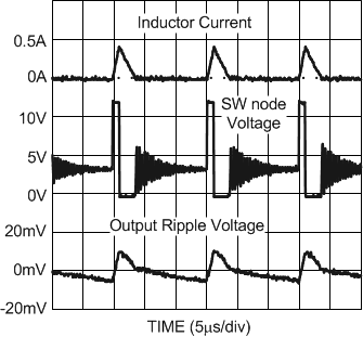
| VIN = 12 V | VOUT = 3.3 V | IOUT = 50 mA |
| L = 22 µH |
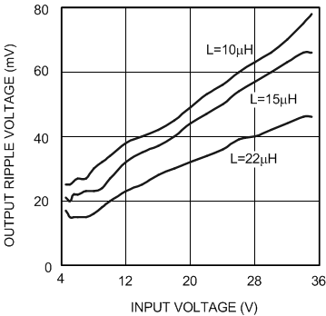
| VOUT = 3.3 V | IOUT = 1 A | COUT(ESR) = 80 mΩ |
| Cff = 100 pF |
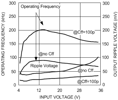
| VOUT = 3.3 V | ||
| L = 22 µH | ||
| IOUT = 500 mA |
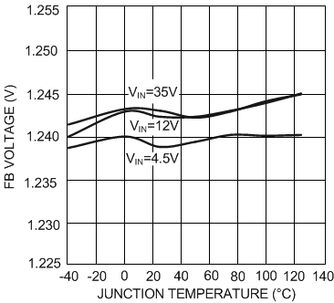
| VIN = 9 V |
| VIN = 4.5 V |
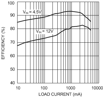
| VOUT = 3.3 V | L = 6.8 µH |
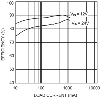
| VOUT = 5.0 V | L = 22 µH |
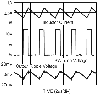
| VIN = 12 V | VOUT = 3.3 V | IOUT = 500 mA |
| L = 22 µH |
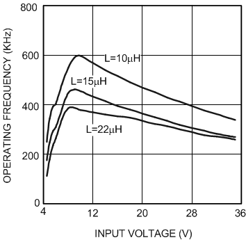
| VOUT = 3.3 V | IOUT = 1 A | COUT(ESR) = 80 mΩ |
| Cff = 100 pF |
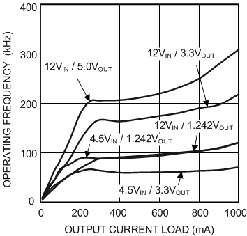
| L = 22 µH | COUT(ESR) = 45 mΩ | Cff = 100 pF |