SNVS178H January 2002 – December 2015 LM3485
PRODUCTION DATA.
- 1 Features
- 2 Applications
- 3 Description
- 4 Revision History
- 5 Pin Configuration and Functions
- 6 Specifications
- 7 Detailed Description
-
8 Application and Implementation
- 8.1 Application Information
- 8.2
Typical Application
- 8.2.1 Design Requirements
- 8.2.2
Detailed Design Procedure
- 8.2.2.1 Step by Step Design Procedure
- 8.2.2.2 Inductor Selection (L1)
- 8.2.2.3 Output Voltage Set Point
- 8.2.2.4 Output Capacitor Selection (COUT)
- 8.2.2.5 Input Capacitor Selection (CIN)
- 8.2.2.6 Programming the Current Limit (RADJ)
- 8.2.2.7 Catch Diode Selection (D1)
- 8.2.2.8 P-Channel MOSFET Selection (Q1)
- 8.2.3 Application Curves
- 9 Power Supply Recommendations
- 10Layout
- 11Device and Documentation Support
- 12Mechanical, Packaging, and Orderable Information
10 Layout
10.1 Layout Guidelines
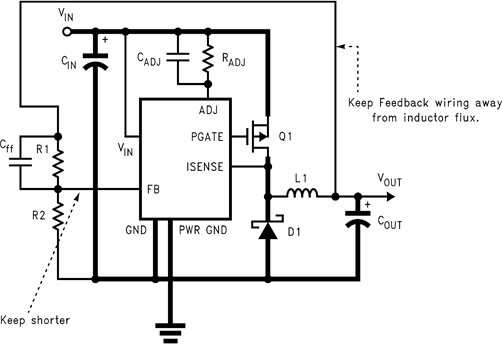
The PC board layout is very important in all switching regulator designs. Poor layout can cause switching noise into the feedback signal and general EMI problems. For minimal inductance, the wires indicated by heavy lines should be as wide and short as possible. Keep the ground pin of the input capacitor as close as possible to the anode of the diode. This path carries a large AC current. The switching node, the node with the diode cathode, inductor, and FET drain, should be kept short. This node is one of the main sources for radiated EMI because it is an AC voltage at the switching frequency. It is always good practice to use a ground plane in the design, particularly at high currents.
The two ground pins, PWR GND and GND, should be connected by as short a trace as possible; they can be connected underneath the device. These pins are resistively connected internally by approximately 50 Ω. The ground pins should be tied to the ground plane, or to a large ground trace in close proximity to both the FB divider and COUT grounds.
The gate pin of the external PFET should be located close to the PGATE pin. However, if a very small FET is used, a resistor may be required between PGATE and the gate of the FET to reduce high frequency ringing. Because this resistor will slow the rise time of the PFET, the current limit blanking time should be taken into consideration (see Current Limit Operation).
The feedback voltage signal line can be sensitive to noise. Avoid inductive coupling to the inductor or the switching node, by keeping the FB trace away from these areas.
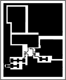
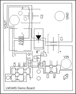
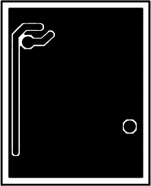
Layout Example
 Figure 30. Top Layer,
 Typical PCB Layout (3.3-V Output)
 Figure 32. Silk Screen,
 Typical PCB Layout (3.3-V Output)
 Figure 31. Bottom Layer,
 Typical PCB Layout (3.3-V Output)
 Figure 33. Typical PCB Layout Schematic (3.3-V Output)