SNVS178H January 2002 – December 2015 LM3485
PRODUCTION DATA.
- 1 Features
- 2 Applications
- 3 Description
- 4 Revision History
- 5 Pin Configuration and Functions
- 6 Specifications
- 7 Detailed Description
-
8 Application and Implementation
- 8.1 Application Information
- 8.2
Typical Application
- 8.2.1 Design Requirements
- 8.2.2
Detailed Design Procedure
- 8.2.2.1 Step by Step Design Procedure
- 8.2.2.2 Inductor Selection (L1)
- 8.2.2.3 Output Voltage Set Point
- 8.2.2.4 Output Capacitor Selection (COUT)
- 8.2.2.5 Input Capacitor Selection (CIN)
- 8.2.2.6 Programming the Current Limit (RADJ)
- 8.2.2.7 Catch Diode Selection (D1)
- 8.2.2.8 P-Channel MOSFET Selection (Q1)
- 8.2.3 Application Curves
- 9 Power Supply Recommendations
- 10Layout
- 11Device and Documentation Support
- 12Mechanical, Packaging, and Orderable Information
7 Detailed Description
7.1 Overview
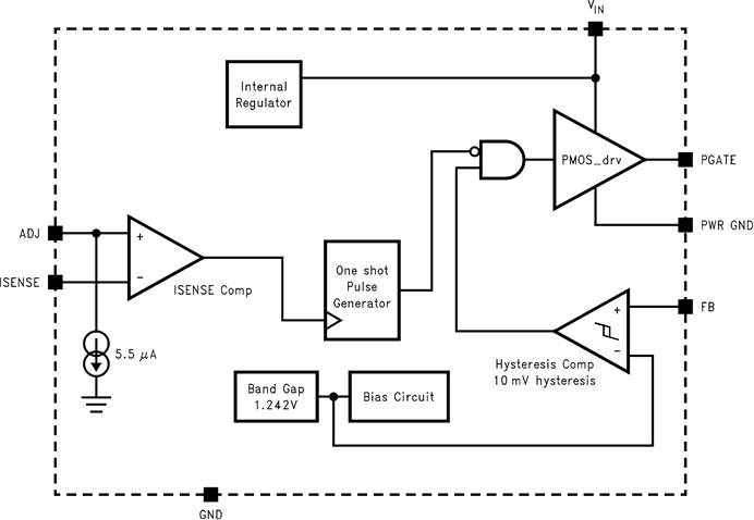
The LM3485 is buck (step-down) DC-DC controller that uses a hysteretic control scheme. The comparator is designed with approximately 10 mV of hysteresis. In response to the voltage at the FB pin, the gate drive (PGATE pin) turns the external PFET on or off. When the inductor current is too high, the current limit protection circuit engages and turns the PFET off for approximately 9 µs.
Hysteretic control does not require an internal oscillator. Switching frequency depends on the external components and operating conditions. Operating frequency reduces at light loads resulting in excellent efficiency compared to other architectures.
Two external resistors can easily program the output voltage. The output can be set in a wide range from
1.242-V (typical) to VIN.
7.2 Functional Block Diagram
7.3 Feature Description
7.3.1 Hysteretic Control Circuit
The LM3485 uses a comparator-based voltage control loop. The feedback is compared to a 1.242-V reference, and a 10-mV hysteresis is designed into the comparator to ensure noise free operation.
When the FB input to the comparator falls below the reference voltage, the output of the comparator moves to a low state. This results in the driver output, PGATE, pulling the gate of the PFET low and turning on the PFET. With the PFET on, the input supply charges Cout and supplies current to the load via the series path through the PFET and the inductor. Current through the Inductor ramps up linearly and the output voltage increases. As the FB voltage reaches the upper threshold, which is the internal reference voltage plus 10 mV, the output of the comparator changes from low to high, and the PGATE responds by turning the PFET off. As the PFET turns off, the inductor voltage reverses, the catch diode turns on, and the current through the inductor ramps down. Then, as the output voltage reaches the internal reference voltage again, the next cycle starts.
The LM3485 operates in discontinuous conduction mode at light load current or continuous conduction mode at heavy load current. In discontinuous conduction mode, current through the inductor starts at zero and ramps up to the peak, then ramps down to zero. Next cycle starts when the FB voltage reaches the internal voltage. Until then, the inductor current remains zero. Operating frequency is lower and switching losses reduce. In continuous conduction mode, current always flows through the inductor and never ramps down to zero.
The output voltage (VOUT) can be programmed by two external resistors. It can be calculated as Equation 1:
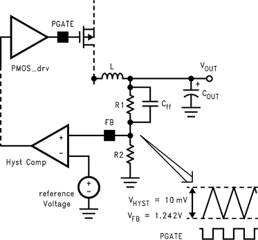 Figure 22. Hysteretic Window
The minimum output voltage ripple (VOUT_PP) can be calculated in the same way.
For example, with VOUT set to 3.3 V, VOUT_PP is 26.6 mV
Operating frequency (F) is determined by knowing the input voltage, output voltage, inductor, VHYST, equivalent series resistance (ESR) of output capacitor, and the delay. It can be approximately calculated using Equation 4:

where
- ( R1 + R2 ) / R2
- delay: It includes the LM3485 propagation delay time and the PFET delay time
The propagation delay is 90-ns typically (see Figure 23).
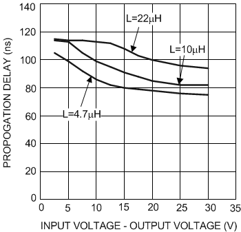 Figure 23. Propagation Delay
The operating frequency and output ripple voltage can also be significantly influenced by the speed up capacitor (Cff). Cff is connected in parallel with the high-side feedback resistor, R1. The location of this capacitor is similar to where a feed-forward capacitor would be located in a PWM control scheme. However, the effect on hysteretic operation is much different. The output ripple causes a current to be sourced or sunk through this capacitor. This current is essentially a square wave. Because the input to the feedback pin, FB, is a high impedance node, the current flows through R2. The end result is a reduction in output ripple and an increase in operating frequency. When adding Cff, calculate Equation 4 with α = 1. The value of Cff depends on the desired operating frequency and the value of R2. A good starting point is 470-pF ceramic at 100-kHz decreasing linearly with increased operating frequency. Also, as the output voltage is programmed below 2.5 V, the effect of Cff will decrease significantly.
7.3.2 Current Limit Operation
The LM3485 has a cycle-by-cycle current limit. Current limit is sensed across the VDS of the PFET or across an additional sense resistor. When current limit is activated, the LM3485 turns off the external PFET for a period of 9 µs (typical). The current limit is adjusted by an external resistor, RADJ.
The current limit circuit is composed of the ISENSE comparator and the one-shot pulse generator. The positive input of the ISENSE comparator is the ADJ pin. An internal 5.5-µA current sink creates a voltage across the external RADJ resistor. This voltage is compared to the voltage across the PFET or sense resistor. The ADJ voltage can be calculated with Equation 5.
where
- 3.0 µA is the minimum ICL-ADJ value
The negative input of the ISENSE comparator is the ISENSE pin that should be connected to the drain of the external PFET. The inductor current is determined by sensing the VDS. It can be calculated with Equation 6.
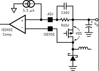 Figure 24. Current Sensing by VDS
The current limit is activated when the voltage at the ADJ pin exceeds the voltage at the ISENSE pin. The ISENSE comparator triggers the 9-µs one shot pulse generator forcing the driver to turn the PFET off. The driver turns the PFET back on after 9 µs. If the current has not reduced below the set threshold, the cycle will repeat continuously.
A filter capacitor, CADJ, should be placed as shown in Figure 24. CADJ filters unwanted noise so that the ISENSE comparator will not be accidentally triggered. A value of 100 pF to 1 nF is recommended in most applications. Higher values can be used to create a soft-start function (see Start Up).
The current limit comparator has approximately 100 ns of blanking time. This ensures that the PFET is fully on when the current is sensed. However, under extreme conditions such as cold temperature, some PFETs may not fully turn on within the blanking time. In this case, the current limit threshold must be increased. If the current limit function is used, the on time must be greater than 100 ns. Under low duty cycle operation, the maximum operating frequency will be limited by this minimum on time.
During current limit operation, the output voltage will drop significantly as will operating frequency. As the load current is reduced, the output will return to the programmed voltage. However, there is a current limit foldback phenomenon inherent in this current limit architecture. See Figure 25.
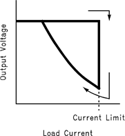 Figure 25. Current Limit Fold Back Phenomenon
At high input voltages (>28 V) increased undershoot at the switch node can cause an increase in the current limit threshold. To avoid this problem, a low Vf Schottky catch diode must be used (see Catch Diode Selection (D1)). Additionally, a resistor can be placed between the ISENSE pin and the switch node. Any value up to approximately 600 Ω is recommended.
7.4 Device Functional Modes
7.4.1 Start Up
The current limit circuit is active during start-up. During start-up the PFET will stay on until either the current limit or the feedback comparator is tripped
If the current limit comparator is tripped first then the fold back characteristic should be taken into account. Start-up into full load may require a higher current limit set point or the load must be applied after start-up.
One problem with selecting a higher current limit is inrush current during start-up. Increasing the capacitance (CADJ) in parallel with RADJ results in soft-start. CADJ and RADJ create an RC time constant forcing current limit to activate at a lower current. The output voltage will ramp more slowly when using the soft-start functionality. There are example start-up plots for CADJ equal to 1 nF and 10 nF in Typical Characteristics. Lower values for CADJ will have little to no effect on soft-start.
7.4.2 External Sense Resistor
The VDS of a PFET will tend to vary significantly over temperature. This will result an equivalent variation in current limit. To improve current limit accuracy an external sense resistor can be connected from VIN to the source of the PFET, as shown in Figure 26.
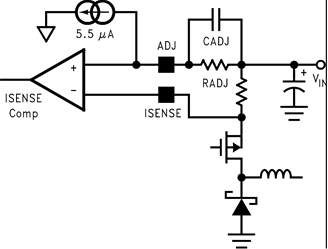 Figure 26. Current Sensing by External Resistor
7.4.3 PGATE
When switching, the PGATE pin swings from VIN (off) to some voltage below VIN (on). How far the PGATE will swing depends on several factors including the capacitance, on time, and input voltage.
As shown in the Typical Characteristics, PGATE voltage swing will increase with decreasing gate capacitance. Although PGATE voltage will typically be around VIN-5 V, with every small gate capacitances, this value can increase to a typical maximum of VIN-8.3 V.
Additionally, PGATE swing voltage will increase as on time increases. During long on times, such as when operating at 100% duty cycle, the PGATE voltage will eventually fall to its maximum voltage of VIN-8.3 V (typical) regardless of the PFET gate capacitance.
The PGATE voltage will not fall below 0.4 V (typical). Therefore, when the input voltage falls below approximately 9 V, the PGATE swing voltage range will be reduced. At an input voltage of 7 V, for instance, PGATE will swing from 7 V to a minimum of 0.4 V.