SNVS603D August 2009 – July 2019 LM3424
PRODUCTION DATA.
- 1 Features
- 2 Applications
- 3 Description
- 4 Revision History
- 5 Pin Configuration and Functions
- 6 Specifications
-
7 Detailed Description
- 7.1 Overview
- 7.2 Functional Block Diagram
- 7.3
Feature Description
- 7.3.1 Current Regulators
- 7.3.2 Peak Current Mode Control
- 7.3.3 Average LED Current
- 7.3.4 Thermal Foldback and Analog Dimming
- 7.3.5 Current Sense and Current Limit
- 7.3.6 Slope Compensation
- 7.3.7 Control Loop Compensation
- 7.3.8 Start-Up Regulator and Soft-Start
- 7.3.9 Overvoltage Lockout (OVLO)
- 7.3.10 Input Undervoltage Lockout (UVLO)
- 7.3.11 PWM Dimming
- 7.3.12 Thermal Shutdown
- 7.4 Device Functional Modes
-
8 Application and Implementation
- 8.1 Application Information
- 8.2
Typical Applications
- 8.2.1
Basic Topology Schematics
- 8.2.1.1 Design Requirements
- 8.2.1.2
Detailed Design Procedure
- 8.2.1.2.1 Operating Point
- 8.2.1.2.2 Switching Frequency
- 8.2.1.2.3 Average LED Current
- 8.2.1.2.4 Thermal Foldback
- 8.2.1.2.5 Inductor Ripple Current
- 8.2.1.2.6 LED Ripple Current
- 8.2.1.2.7 Peak Current Limit
- 8.2.1.2.8 Slope Compensation
- 8.2.1.2.9 Loop Compensation
- 8.2.1.2.10 Input Capacitance
- 8.2.1.2.11 NFET
- 8.2.1.2.12 Diode
- 8.2.1.2.13 Output OVLO
- 8.2.1.2.14 Input UVLO
- 8.2.1.2.15 Soft-Start
- 8.2.1.2.16 PWM Dimming Method
- 8.2.1.2.17 Analog Dimming Method
- 8.2.2
Buck-Boost Application
- 8.2.2.1 Design Requirements
- 8.2.2.2
Detailed Design Procedure
- 8.2.2.2.1 Operating Point
- 8.2.2.2.2 Switching Frequency
- 8.2.2.2.3 Average LED Current
- 8.2.2.2.4 Thermal Foldback
- 8.2.2.2.5 Inductor Ripple Current
- 8.2.2.2.6 Output Capacitance
- 8.2.2.2.7 Peak Current Limit
- 8.2.2.2.8 Slope Compensation
- 8.2.2.2.9 Loop Compensation
- 8.2.2.2.10 Input Capacitance
- 8.2.2.2.11 NFET
- 8.2.2.2.12 Diode
- 8.2.2.2.13 Input UVLO
- 8.2.2.2.14 Output OVLO
- 8.2.2.2.15 Soft-Start
- 8.2.2.3 Application Curve
- 8.2.3 Boost Application
- 8.2.4 Buck-Boost Application
- 8.2.5 Boost Application
- 8.2.6 Buck-Boost Application
- 8.2.7 Buck Application
- 8.2.8 Buck-Boost Application
- 8.2.9 SEPIC Application
- 8.2.1
Basic Topology Schematics
- 9 Power Supply Recommendations
- 10Layout
- 11Device and Documentation Support
- 12Mechanical, Packaging, and Orderable Information
7.3.8 Start-Up Regulator and Soft-Start
The LM3424 includes a high voltage, low dropout bias regulator. When power is applied, the regulator is enabled and sources current into an external capacitor (CBYP) connected to the VCC pin. The recommended bypass capacitance for the VCC regulator is 2.2 µF to 3.3 µF. The output of the VCC regulator is monitored by an internal UVLO circuit that protects the device from attempting to operate with insufficient supply voltage and the supply is also internally current limited.
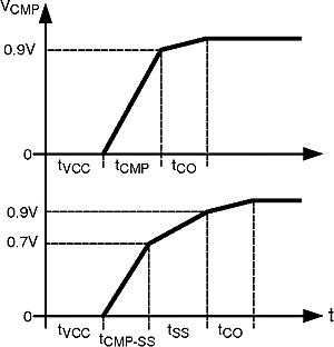
The LM3424 also has programmable soft-start, set by an external capacitor (CSS), connected from SS to GND. For CSS to affect start-up, CREF > CNTC must be maintained so that the converter does not start in foldback mode. Figure 27 shows the typical start-up waveforms for the LM3424 assuming CREF > CNTC.
 Figure 27. Start-up Waveforms
 First, CBYP is charged to be above VCC UVLO threshold (~4.2V). The CVCC charging time (tVCC) can be estimated as:

Assuming there is no CSS or if CSS is less than 40% of CCMP , CCMP is then charged to 0.9V over the charging time (tCMP) which can be estimated as:

Once CCMP = 0.9V, the part starts switching to charge CO until the LED current is in regulation. The CO charging time (tCO) can be roughly estimated as:

If CSS is greater than 40% of CCMP, the compensation capacitor will only charge to 0.7V over a smaller CCMP charging time (tCMP-SS) which can be estimated as:

Then COMP will clamp to SS, forcing COMP to rise (the last 200 mV before switching begins) according to the CSS charging time (tSS) which can be estimated as:

The system start-up time (tSU or tSU-SS) is defined as:
CSS < 0.4 x CCMP

CSS > 0.4 x CCMP

As a general rule of thumb, standard smooth startup operation can be achieved with CSS = CCMP.