SNVS603D August 2009 – July 2019 LM3424
PRODUCTION DATA.
- 1 Features
- 2 Applications
- 3 Description
- 4 Revision History
- 5 Pin Configuration and Functions
- 6 Specifications
-
7 Detailed Description
- 7.1 Overview
- 7.2 Functional Block Diagram
- 7.3
Feature Description
- 7.3.1 Current Regulators
- 7.3.2 Peak Current Mode Control
- 7.3.3 Average LED Current
- 7.3.4 Thermal Foldback and Analog Dimming
- 7.3.5 Current Sense and Current Limit
- 7.3.6 Slope Compensation
- 7.3.7 Control Loop Compensation
- 7.3.8 Start-Up Regulator and Soft-Start
- 7.3.9 Overvoltage Lockout (OVLO)
- 7.3.10 Input Undervoltage Lockout (UVLO)
- 7.3.11 PWM Dimming
- 7.3.12 Thermal Shutdown
- 7.4 Device Functional Modes
-
8 Application and Implementation
- 8.1 Application Information
- 8.2
Typical Applications
- 8.2.1
Basic Topology Schematics
- 8.2.1.1 Design Requirements
- 8.2.1.2
Detailed Design Procedure
- 8.2.1.2.1 Operating Point
- 8.2.1.2.2 Switching Frequency
- 8.2.1.2.3 Average LED Current
- 8.2.1.2.4 Thermal Foldback
- 8.2.1.2.5 Inductor Ripple Current
- 8.2.1.2.6 LED Ripple Current
- 8.2.1.2.7 Peak Current Limit
- 8.2.1.2.8 Slope Compensation
- 8.2.1.2.9 Loop Compensation
- 8.2.1.2.10 Input Capacitance
- 8.2.1.2.11 NFET
- 8.2.1.2.12 Diode
- 8.2.1.2.13 Output OVLO
- 8.2.1.2.14 Input UVLO
- 8.2.1.2.15 Soft-Start
- 8.2.1.2.16 PWM Dimming Method
- 8.2.1.2.17 Analog Dimming Method
- 8.2.2
Buck-Boost Application
- 8.2.2.1 Design Requirements
- 8.2.2.2
Detailed Design Procedure
- 8.2.2.2.1 Operating Point
- 8.2.2.2.2 Switching Frequency
- 8.2.2.2.3 Average LED Current
- 8.2.2.2.4 Thermal Foldback
- 8.2.2.2.5 Inductor Ripple Current
- 8.2.2.2.6 Output Capacitance
- 8.2.2.2.7 Peak Current Limit
- 8.2.2.2.8 Slope Compensation
- 8.2.2.2.9 Loop Compensation
- 8.2.2.2.10 Input Capacitance
- 8.2.2.2.11 NFET
- 8.2.2.2.12 Diode
- 8.2.2.2.13 Input UVLO
- 8.2.2.2.14 Output OVLO
- 8.2.2.2.15 Soft-Start
- 8.2.2.3 Application Curve
- 8.2.3 Boost Application
- 8.2.4 Buck-Boost Application
- 8.2.5 Boost Application
- 8.2.6 Buck-Boost Application
- 8.2.7 Buck Application
- 8.2.8 Buck-Boost Application
- 8.2.9 SEPIC Application
- 8.2.1
Basic Topology Schematics
- 9 Power Supply Recommendations
- 10Layout
- 11Device and Documentation Support
- 12Mechanical, Packaging, and Orderable Information
7.3.7 Control Loop Compensation
The LM3424 control loop is modeled like any current mode controller. Using a first order approximation, the uncompensated loop can be modeled as a single pole created by the output capacitor and, in the boost and buck-boost topologies, a right half plane zero created by the inductor, where both have a dependence on the LED string dynamic resistance. There is also a high frequency pole in the model, however it is near the switching frequency and plays no part in the compensation design process therefore it will be neglected. Since ceramic capacitance is recommended for use with LED drivers due to long lifetimes and high ripple current rating, the ESR of the output capacitor can also be neglected in the loop analysis. Finally, there is a DC gain of the uncompensated loop which is dependent on internal controller gains and the external sensing network.
A buck-boost regulator will be used as an example case. See the Application Information section for compensation of all topologies.
The uncompensated loop gain for a buck-boost regulator is given by the following equation:
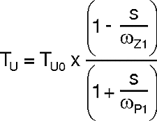
Where the uncompensated DC loop gain of the system is described as:

And the output pole (ωP1) is approximated:

And the right half plane zero (ωZ1) is:

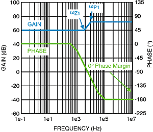 Figure 24. Uncompensated Loop Gain Frequency Response
 Figure 24 shows the uncompensated loop gain in a worst-case scenario when the RHP zero is below the output pole. This occurs at high duty cycles when the regulator is trying to boost the output voltage significantly. The RHP zero adds 20dB/decade of gain while loosing 45°/decade of phase which places the crossover frequency (when the gain is zero dB) extremely high because the gain only starts falling again due to the high frequency pole (not modeled or shown in figure). The phase will be below -180° at the crossover frequency which means there is no phase margin (180° + phase at crossover frequency) causing system instability. Even if the output pole is below the RHP zero, the phase will still reach -180° before the crossover frequency in most cases yielding instability.
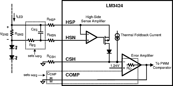 Figure 25. Compensation Circuitry
 To mitigate this problem, a compensator should be designed to give adequate phase margin (above 45°) at the crossover frequency. A simple compensator using a single capacitor at the COMP pin (CCMP) will add a dominant pole to the system, which will ensure adequate phase margin if placed low enough. At high duty cycles (as shown in Figure 24), the RHP zero places extreme limits on the achievable bandwidth with this type of compensation. However, because an LED driver is essentially free of output transients (except catastrophic failures open or short), the dominant pole approach, even with reduced bandwidth, is usually the best approach. The dominant compensation pole (ωP2) is determined by CCMP and the output resistance (RO) of the error amplifier (typically 5 MΩ):

It may also be necessary to add one final pole at least one decade above the crossover frequency to attenuate switching noise and, in some cases, provide better gain margin. This pole can be placed across RSNS to filter the ESL of the sense resistor at the same time. Figure 25 shows how the compensation is physically implemented in the system.
The high frequency pole (ωP3) can be calculated:

The total system transfer function becomes:
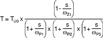
The resulting compensated loop gain frequency response shown in Figure 26 indicates that the system has adequate phase margin (above 45°) if the dominant compensation pole is placed low enough, ensuring stability:
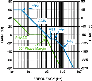 Figure 26. Compensated Loop Gain Frequency Response