SNVS603D August 2009 – July 2019 LM3424
PRODUCTION DATA.
- 1 Features
- 2 Applications
- 3 Description
- 4 Revision History
- 5 Pin Configuration and Functions
- 6 Specifications
-
7 Detailed Description
- 7.1 Overview
- 7.2 Functional Block Diagram
- 7.3
Feature Description
- 7.3.1 Current Regulators
- 7.3.2 Peak Current Mode Control
- 7.3.3 Average LED Current
- 7.3.4 Thermal Foldback and Analog Dimming
- 7.3.5 Current Sense and Current Limit
- 7.3.6 Slope Compensation
- 7.3.7 Control Loop Compensation
- 7.3.8 Start-Up Regulator and Soft-Start
- 7.3.9 Overvoltage Lockout (OVLO)
- 7.3.10 Input Undervoltage Lockout (UVLO)
- 7.3.11 PWM Dimming
- 7.3.12 Thermal Shutdown
- 7.4 Device Functional Modes
-
8 Application and Implementation
- 8.1 Application Information
- 8.2
Typical Applications
- 8.2.1
Basic Topology Schematics
- 8.2.1.1 Design Requirements
- 8.2.1.2
Detailed Design Procedure
- 8.2.1.2.1 Operating Point
- 8.2.1.2.2 Switching Frequency
- 8.2.1.2.3 Average LED Current
- 8.2.1.2.4 Thermal Foldback
- 8.2.1.2.5 Inductor Ripple Current
- 8.2.1.2.6 LED Ripple Current
- 8.2.1.2.7 Peak Current Limit
- 8.2.1.2.8 Slope Compensation
- 8.2.1.2.9 Loop Compensation
- 8.2.1.2.10 Input Capacitance
- 8.2.1.2.11 NFET
- 8.2.1.2.12 Diode
- 8.2.1.2.13 Output OVLO
- 8.2.1.2.14 Input UVLO
- 8.2.1.2.15 Soft-Start
- 8.2.1.2.16 PWM Dimming Method
- 8.2.1.2.17 Analog Dimming Method
- 8.2.2
Buck-Boost Application
- 8.2.2.1 Design Requirements
- 8.2.2.2
Detailed Design Procedure
- 8.2.2.2.1 Operating Point
- 8.2.2.2.2 Switching Frequency
- 8.2.2.2.3 Average LED Current
- 8.2.2.2.4 Thermal Foldback
- 8.2.2.2.5 Inductor Ripple Current
- 8.2.2.2.6 Output Capacitance
- 8.2.2.2.7 Peak Current Limit
- 8.2.2.2.8 Slope Compensation
- 8.2.2.2.9 Loop Compensation
- 8.2.2.2.10 Input Capacitance
- 8.2.2.2.11 NFET
- 8.2.2.2.12 Diode
- 8.2.2.2.13 Input UVLO
- 8.2.2.2.14 Output OVLO
- 8.2.2.2.15 Soft-Start
- 8.2.2.3 Application Curve
- 8.2.3 Boost Application
- 8.2.4 Buck-Boost Application
- 8.2.5 Boost Application
- 8.2.6 Buck-Boost Application
- 8.2.7 Buck Application
- 8.2.8 Buck-Boost Application
- 8.2.9 SEPIC Application
- 8.2.1
Basic Topology Schematics
- 9 Power Supply Recommendations
- 10Layout
- 11Device and Documentation Support
- 12Mechanical, Packaging, and Orderable Information
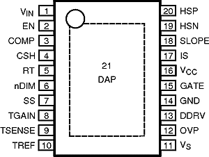
5 Pin Configuration and Functions
PWP Package
20-Pin HTSSOP With PowerPAD™
Top View

Pin Functions
| PIN | I/O | DESCRIPTION | ||
|---|---|---|---|---|
| NO. | NAME | |||
| 1 | VIN | I | Input Voltage | Bypass with 100 nF capacitor to GND as close to the device as possible. |
| 2 | EN | I | Enable | Connect to > 2.4V to enable the device or to < 0.8V for low power shutdown. |
| 3 | COMP | I | Compensation | Connect a capacitor to GND to compensate control loop. |
| 4 | CSH | I | Current Sense High | Connect a resistor to GND to set the signal current. Can also be used to analog dim as explained in the Thermal Foldback and Analog Dimming section. |
| 5 | RT | I | Resistor Timing | Connect a resistor to GND to set the switching frequency. Can also be used to synchronize to an external clock as explained in the Switching Frequency section. |
| 6 | nDIM | I | Dimming Input /
Under-Voltage Protection |
Connect a PWM signal for dimming as detailed in the PWM Dimming section and/or a resistor divider from VIN to program input under-voltage lockout. |
| 7 | SS | I | Soft-start | Connect a capacitor to GND to extend start-up time. |
| 8 | TGAIN | I | Temp Foldback Gain | Connect a resistor to GND to set the foldback slope. |
| 9 | TSENSE | I | Temp Sense Input | Connect a resistor/ thermistor divider from VS to sense the temperature as explained in the Thermal Foldback and Analog Dimming section. |
| 10 | TREF | I | Temp Foldback Reference | Connect a resistor divider from VS to set the foldback reference voltage. |
| 11 | VS | O | Voltage Reference | 2.45V reference for temperature foldback circuit and other external circuitry. |
| 12 | OVP | I | Over-Voltage Protection | Connect a resistor divider from VO to program output over-voltage lockout. |
| 13 | DDRV | O | Dimming Gate Drive Output | Connect to gate of dimming MOSFET. |
| 14 | GND | GND | Ground | Connect to DAP to provide proper system GND |
| 15 | GATE | O | Main Gate Drive Output | Connect to gate of main switching MOSFET. |
| 16 | VCC | O | Internal Regulator Output | Bypass with a 2.2 µF – 3.3 µF ceramic capacitor to GND. |
| 17 | IS | I | Main Switch Current Sense | Connect to the drain of the main N-channel MOSFET switch for RDS-ON sensing or to a sense resistor installed in the source of the same device. |
| 18 | SLOPE | I | Slope Compensation | Connect a resistor to GND to set slope of additional ramp. |
| 19 | HSN | I | LED Current Sense Negative | Connect through a series resistor to LED current sense resistor (negative). |
| 20 | HSP | I | LED Current Sense Positive | Connect through a series resistor to LED current sense resistor (positive). |
| DAP | DAP | GND | Thermal pad on bottom of IC | Connect to GND. |