ZHCSJK1G November 2002 – May 2019 LM2733
PRODUCTION DATA.
- 1 特性
- 2 应用
- 3 说明
- 4 修订历史记录
- 5 Pin Configuration and Functions
- 6 Specifications
- 7 Detailed Description
-
8 Application and Implementation
- 8.1 Application Information
- 8.2
Typical Application
- 8.2.1 Design Requirements
- 8.2.2
Detailed Design Procedure
- 8.2.2.1 Selecting the External Capacitors
- 8.2.2.2 Selecting the Output Capacitor
- 8.2.2.3 Selecting the Input Capacitor
- 8.2.2.4 Feedforward Compensation
- 8.2.2.5 Selecting Diodes
- 8.2.2.6 Setting the Output Voltage
- 8.2.2.7 Switching Frequency
- 8.2.2.8 Duty Cycle
- 8.2.2.9 Inductance Value
- 8.2.2.10 Maximum Switch Current
- 8.2.2.11 Calculating Load Current
- 8.2.2.12 Design Parameters VSW and ISW
- 8.2.2.13 Thermal Considerations
- 8.2.2.14 Minimum Inductance
- 8.2.2.15 Inductor Suppliers
- 8.2.3 Application Curves
- 9 Power Supply Recommendations
- 10Layout
- 11器件和文档支持
- 12机械、封装和可订购信息
8.2.2.9 Inductance Value
The first question we are usually asked is: “How small can I make the inductor?” (because they are the largest sized component and usually the most costly). The answer is not simple and involves tradeoffs in performance. Larger inductors mean less inductor ripple current, which typically means less output voltage ripple (for a given size of output capacitor). Larger inductors also mean more load power can be delivered because the energy stored during each switching cycle is:
Where “lp” is the peak inductor current. An important point to observe is that the LM2733 device will limit its switch current based on peak current. This means that since lp (maximum) is fixed, increasing L will increase the maximum amount of power available to the load. Conversely, using too little inductance may limit the amount of load current which can be drawn from the output.
Best performance is usually obtained when the converter is operated in “continuous” mode at the load current range of interest, typically giving better load regulation and less output ripple. Continuous operation is defined as not allowing the inductor current to drop to zero during the cycle. It should be noted that all boost converters shift over to discontinuous operation as the output load is reduced far enough, but a larger inductor stays “continuous” over a wider load current range.
To better understand these tradeoffs, a typical application circuit (5V to 12V boost with a 10 µH inductor) will be analyzed. We will assume:
VIN = 5 V, VOUT = 12 V, VDIODE = 0.5 V, VSW = 0.5 V
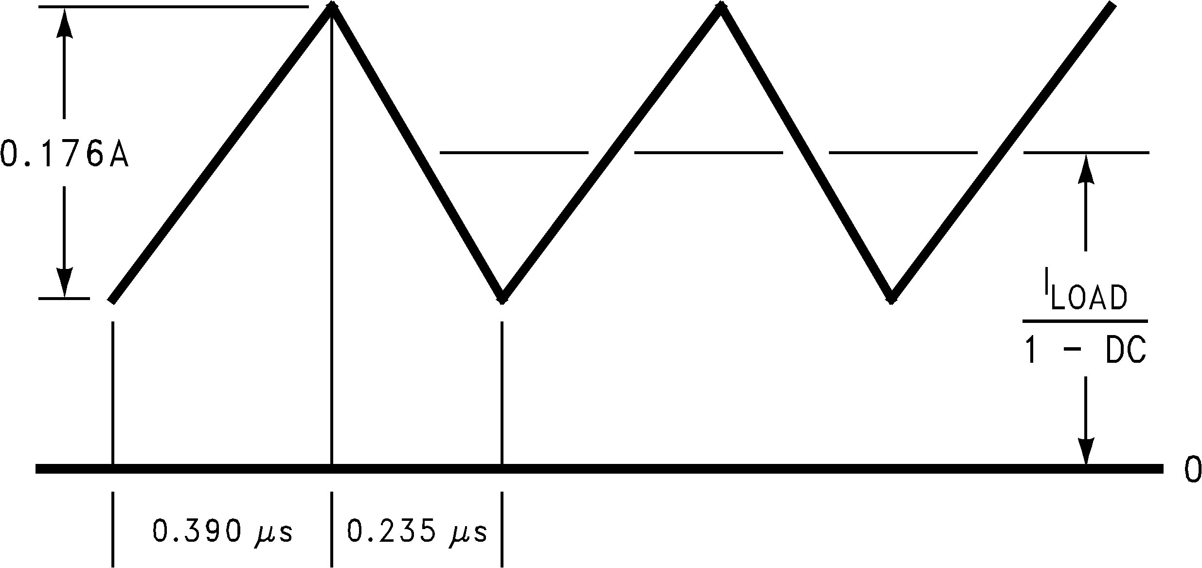
Since the frequency is 1.6 MHz (nominal), the period is approximately 0.625 µs. The duty cycle will be 62.5%, which means the ON time of the switch is 0.390 µs. It should be noted that when the switch is ON, the voltage across the inductor is approximately 4.5 V.
Using the equation:
We can then calculate the di/dt rate of the inductor which is found to be 0.45 A/µs during the ON time. Using these facts, we can then show what the inductor current will look like during operation:
 Figure 25. 10-µH Inductor Current,
5-V – 12-V Boost (LM2733X)
During the 0.390 µs ON time, the inductor current ramps up 0.176 A and ramps down an equal amount during the OFF time. This is defined as the inductor “ripple current”. It can also be seen that if the load current drops to about 33 mA, the inductor current will begin touching the zero axis which means it will be in discontinuous mode. A similar analysis can be performed on any boost converter, to make sure the ripple current is reasonable and continuous operation will be maintained at the typical load current values.