ZHCSJK1G November   2002  – May 2019 LM2733

PRODUCTION DATA.  

  1. 特性
  2. 应用
  3. 说明
    1.     Device Images
      1.      典型应用电路
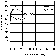
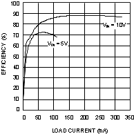
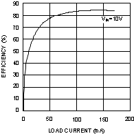
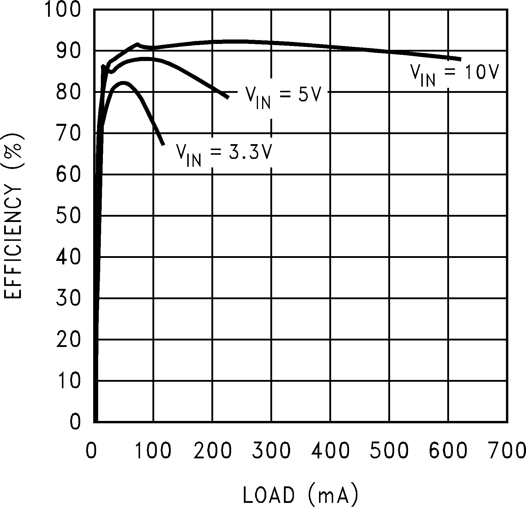
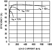
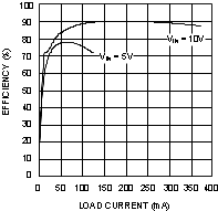
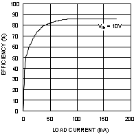
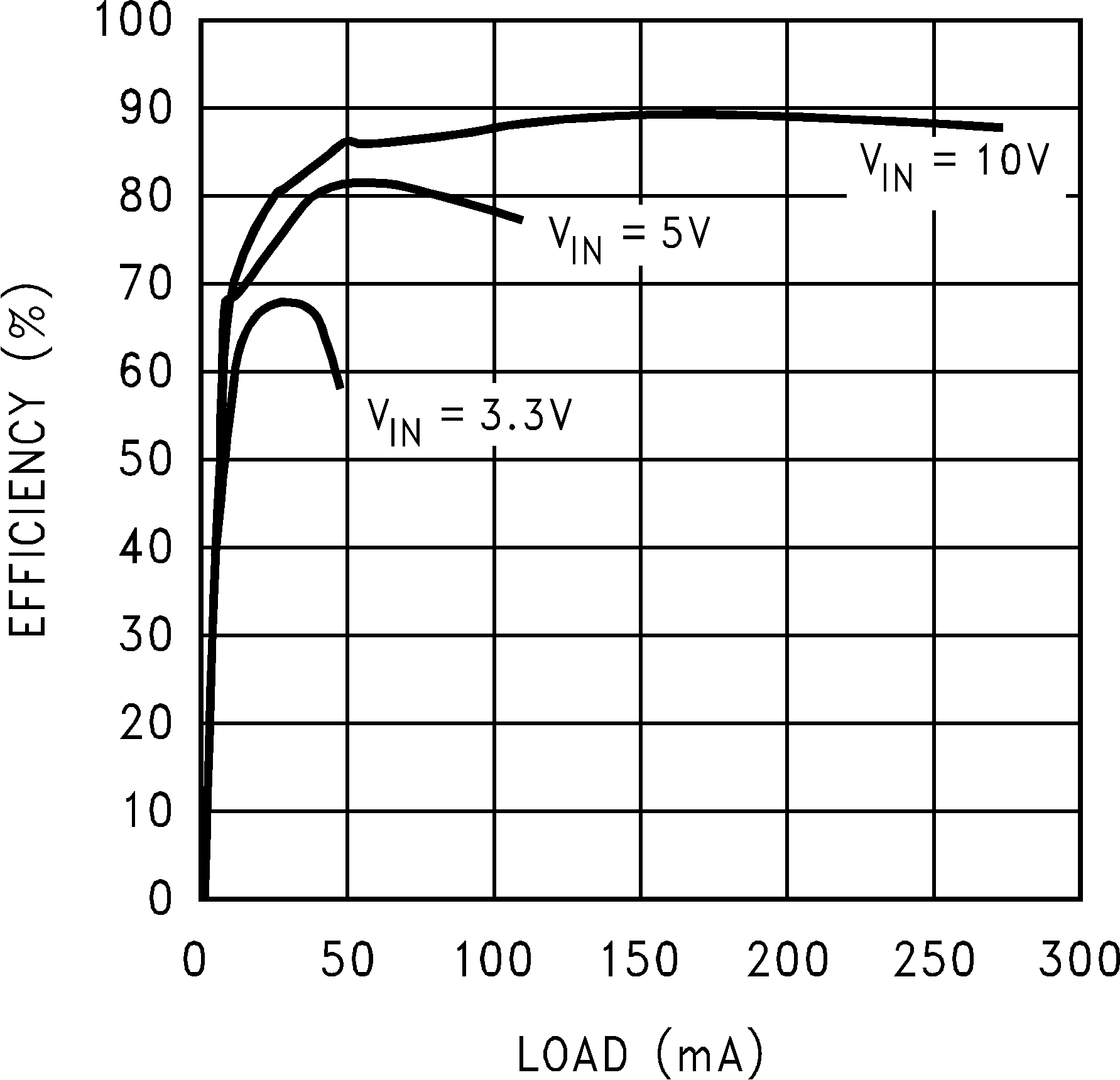
      2.      效率与负载电流间的关系
  4. 修订历史记录
  5. Pin Configuration and Functions
    1.     Pin Functions
  6. Specifications
    1. 6.1 Absolute Maximum Ratings
    2. 6.2 ESD Ratings
    3. 6.3 Recommended Operating Conditions
    4. 6.4 Thermal Information
    5. 6.5 Electrical Characteristics
    6. 6.6 Typical Characteristics
  7. Detailed Description
    1. 7.1 Overview
    2. 7.2 Functional Block Diagram
    3. 7.3 Feature Description
      1. 7.3.1 Switching Frequency
    4. 7.4 Device Functional Modes
      1. 7.4.1 Shutdown Pin Operation
  8. Application and Implementation
    1. 8.1 Application Information
    2. 8.2 Typical Application
      1. 8.2.1 Design Requirements
      2. 8.2.2 Detailed Design Procedure
        1. 8.2.2.1  Selecting the External Capacitors
        2. 8.2.2.2  Selecting the Output Capacitor
        3. 8.2.2.3  Selecting the Input Capacitor
        4. 8.2.2.4  Feedforward Compensation
        5. 8.2.2.5  Selecting Diodes
        6. 8.2.2.6  Setting the Output Voltage
        7. 8.2.2.7  Switching Frequency
        8. 8.2.2.8  Duty Cycle
        9. 8.2.2.9  Inductance Value
        10. 8.2.2.10 Maximum Switch Current
        11. 8.2.2.11 Calculating Load Current
        12. 8.2.2.12 Design Parameters VSW and ISW
        13. 8.2.2.13 Thermal Considerations
        14. 8.2.2.14 Minimum Inductance
        15. 8.2.2.15 Inductor Suppliers
      3. 8.2.3 Application Curves
  9. Power Supply Recommendations
  10. 10Layout
    1. 10.1 Layout Guidelines
    2. 10.2 Layout Example
  11. 11器件和文档支持
    1. 11.1 商标
    2. 11.2 静电放电警告
    3. 11.3 Glossary
  12. 12机械、封装和可订购信息

封装选项

机械数据 (封装 | 引脚)
散热焊盘机械数据 (封装 | 引脚)
订购信息

Typical Characteristics

Unless otherwise specified: VIN = 5 V, SHDN pin is tied to VIN.
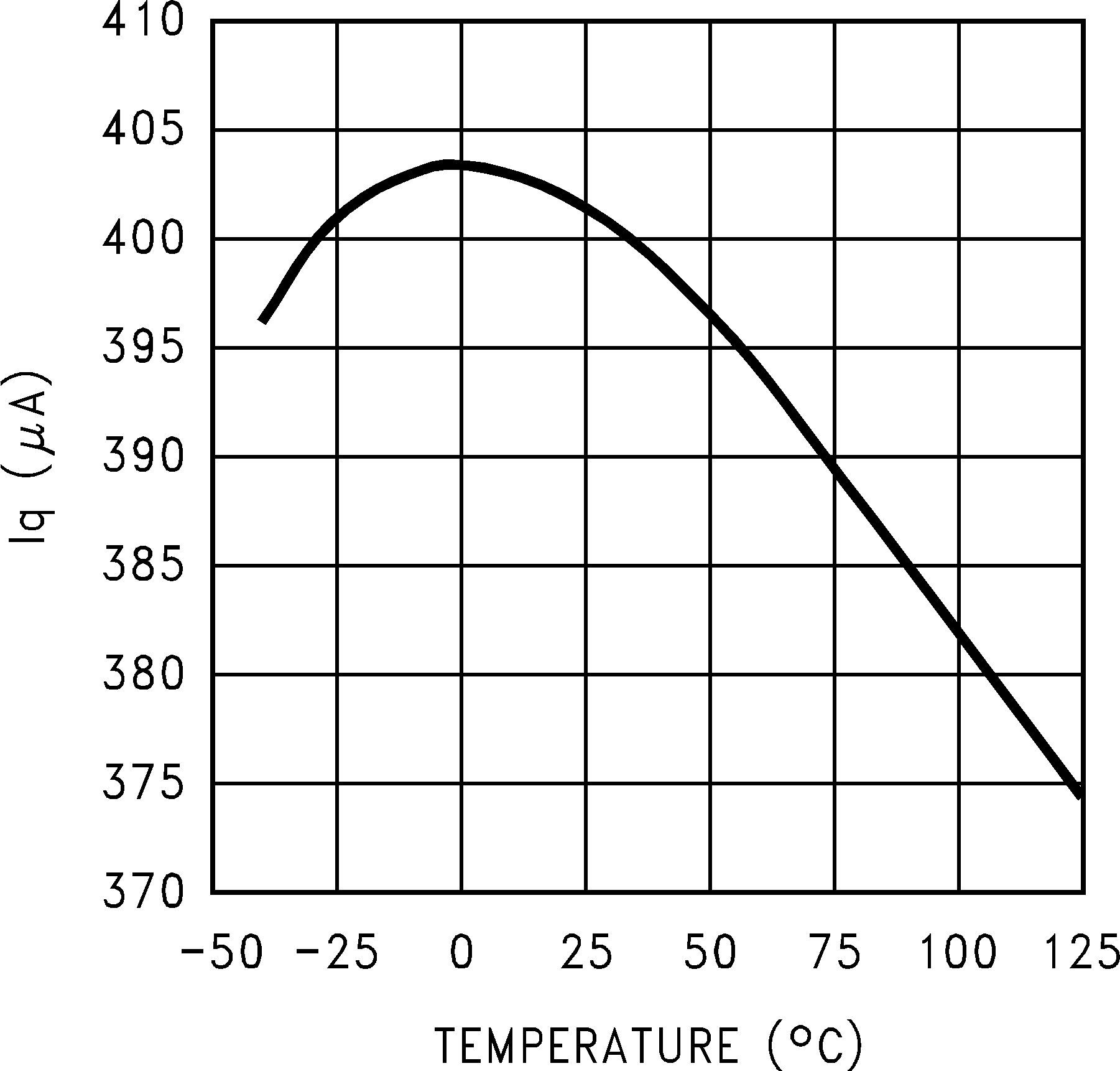
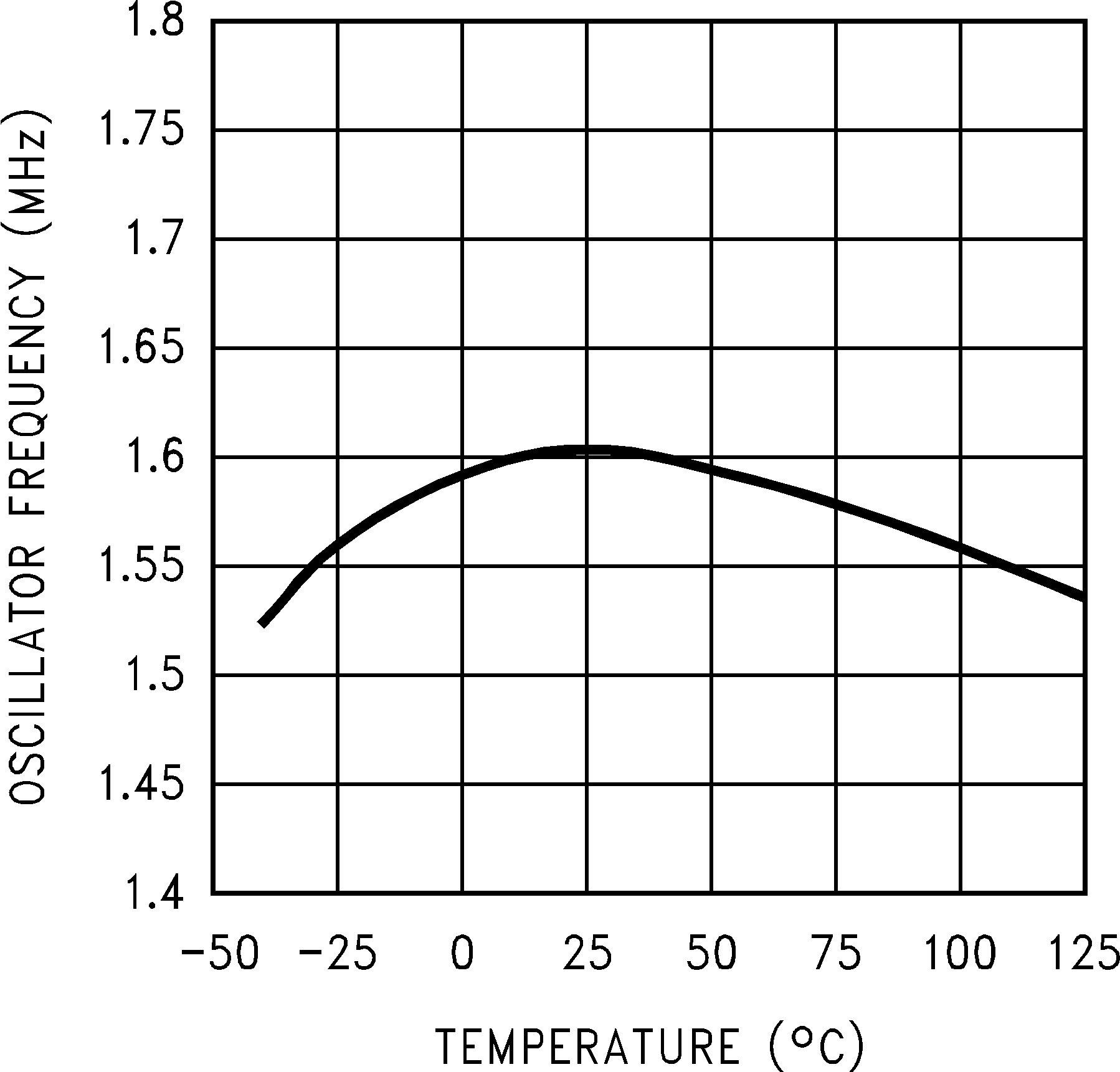
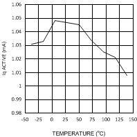
LM2733 20055410.png
Figure 1. Iq VIN (Active) vs Temperature - "X"
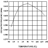
LM2733 20055408.png
Figure 3. Oscillator Frequency vs Temperature - "X"
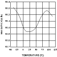
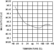
LM2733 20055455.gif
Figure 5. Max. Duty Cycle vs Temperature - "X"
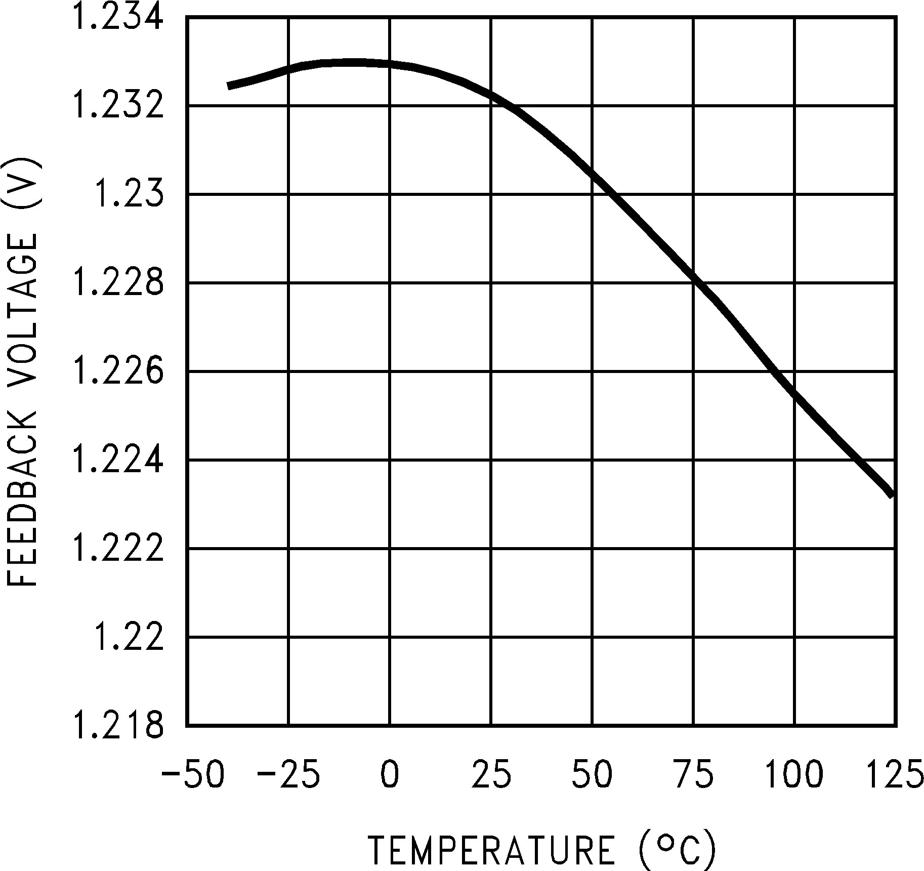
LM2733 20055406.png
Figure 7. Feedback Voltage vs Temperature
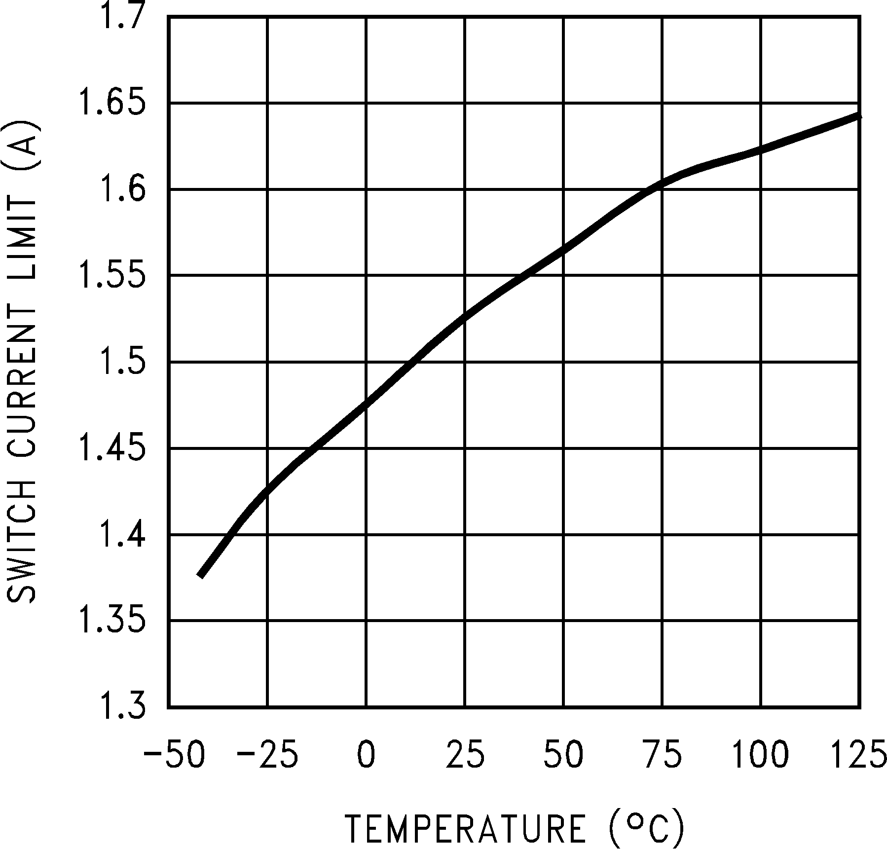
LM2733 20055409.png
Figure 9. Current Limit vs Temperature
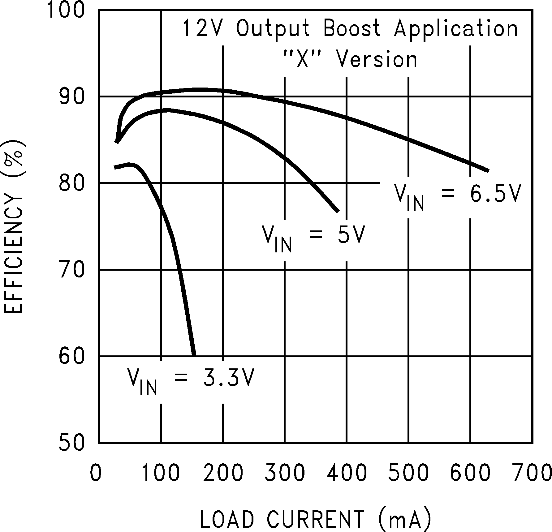
LM2733 20055414.png
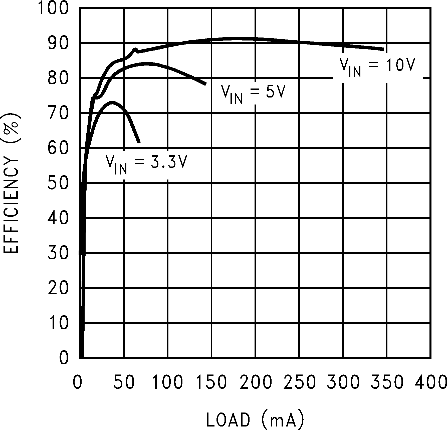
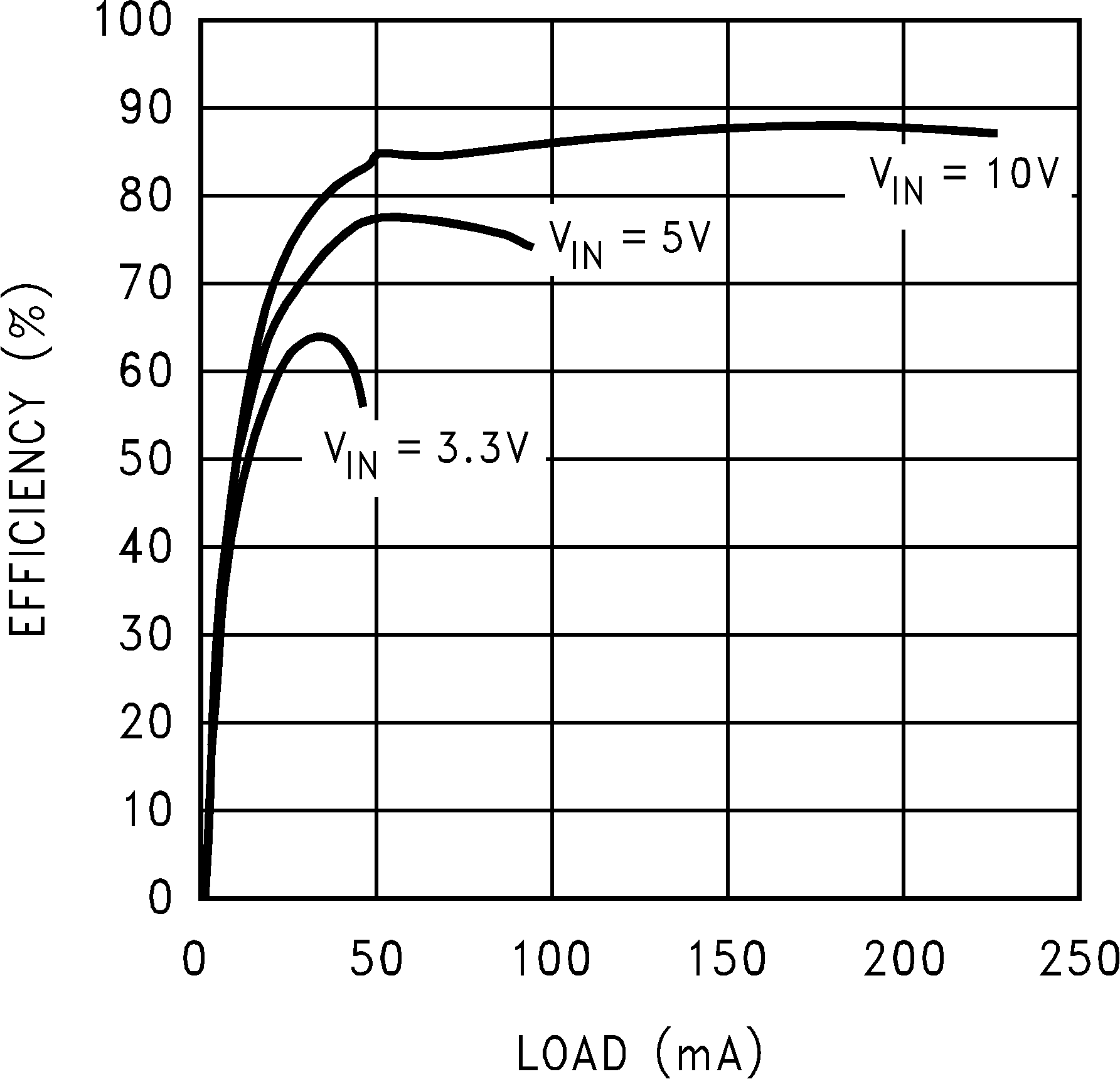
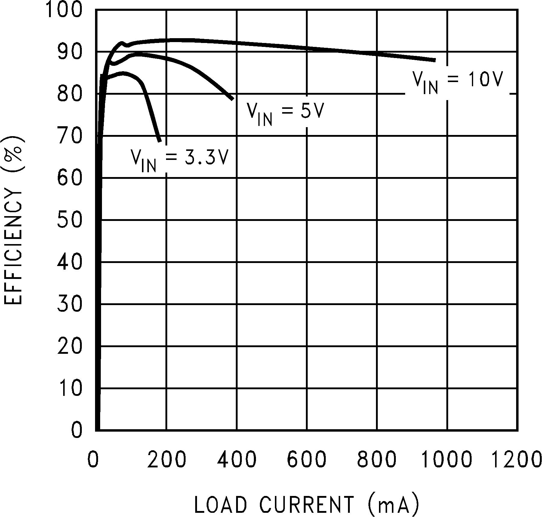
Figure 11. Efficiency vs Load Current (VOUT = 12 V) - "X"
LM2733 20055446.gif
Figure 13. Efficiency vs Load Current (VOUT = 20 V) - "X"
LM2733 20055448.gif
Figure 15. Efficiency vs Load Current (VOUT = 30 V) - "X"
LM2733 20055450.gif
Figure 17. Efficiency vs Load Current (VOUT = 40 V) - "X"
LM2733 20055427.png
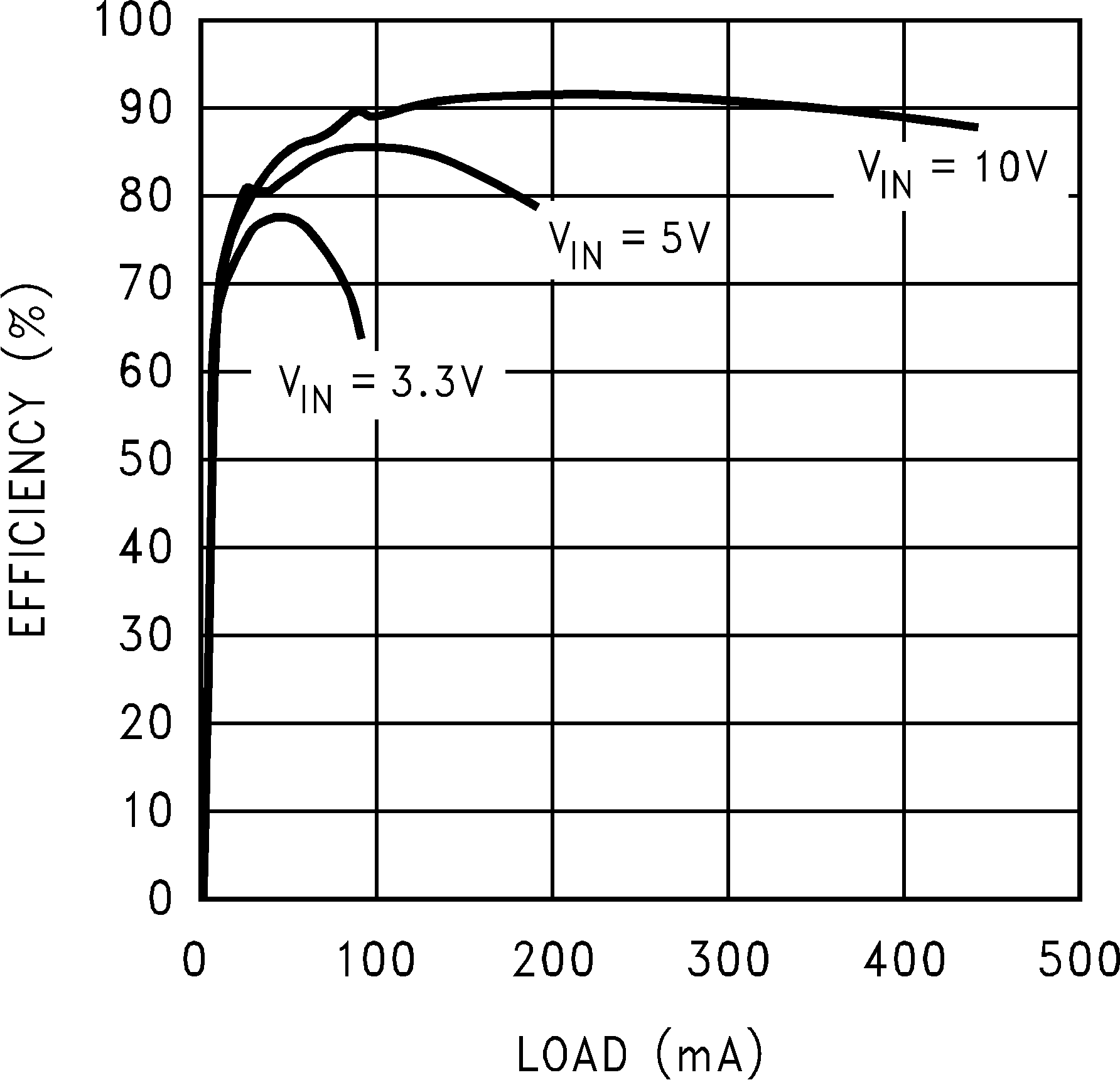
Figure 19. Efficiency vs Load (VOUT = 20 V) - "Y"
LM2733 20055429.png
Figure 21. Efficiency vs Load (VOUT = 30 V) - "Y"
LM2733 20055432.png
Figure 23. Efficiency vs Load (VOUT = 40 V) - "Y"
LM2733 20055442.gif
Figure 2. Iq VIN (Active) vs Temperature - "Y"
LM2733 20055443.gif
Figure 4. Oscillator Frequency vs Temperature - "Y"
LM2733 20055456.gif
Figure 6. Max. Duty Cycle vs Temperature - "Y"
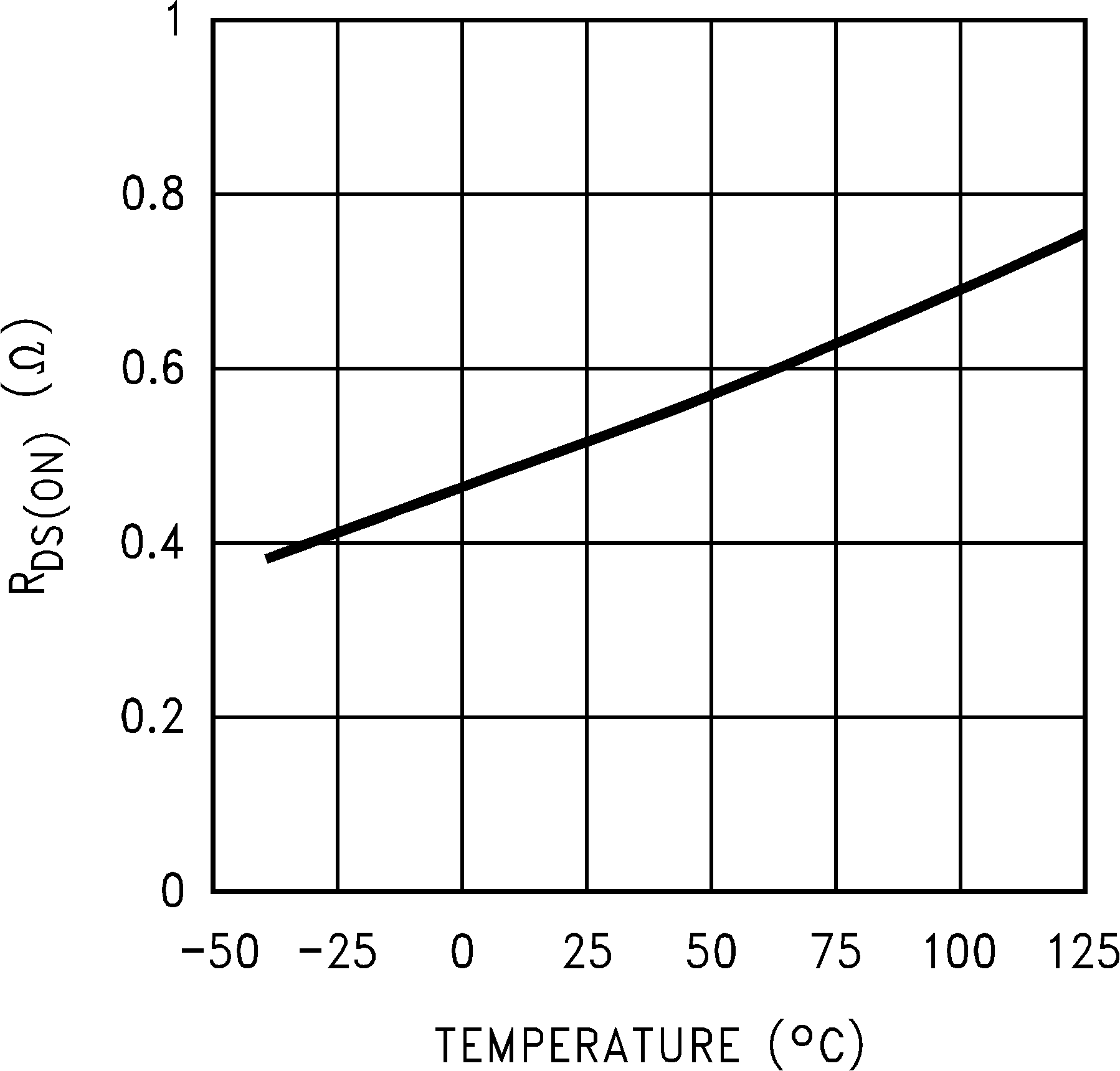
LM2733 20055407.png
Figure 8. RDS(ON) vs Temperature
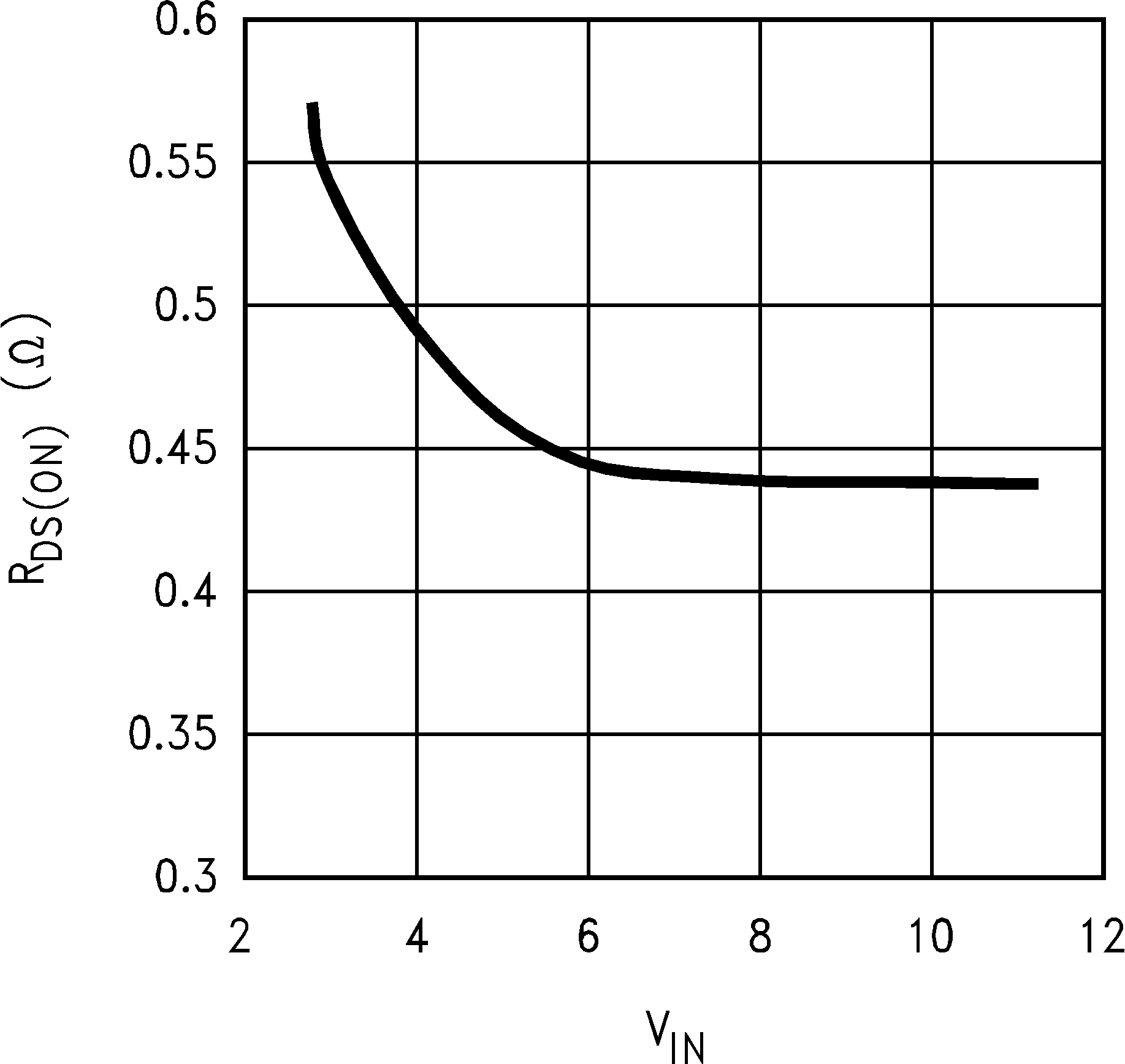
LM2733 20055423.png
Figure 10. RDS(ON) vs VIN
LM2733 20055445.gif
Figure 12. Efficiency vs Load Current (VOUT = 15 V) - "X"
LM2733 20055447.gif
Figure 14. Efficiency vs Load Current (VOUT = 25 V) - "X"
LM2733 20055449.gif
Figure 16. Efficiency vs Load Current (VOUT = 35 V) - "X"
LM2733 20055435.png
Figure 18. Efficiency vs Load (VOUT = 15 V) - "Y"
LM2733 20055428.png
Figure 20. Efficiency vs Load (VOUT = 25 V) - "Y"
LM2733 20055430.png
Figure 22. Efficiency vs Load (VOUT = 35 V) - "Y"