ZHCSLO5B December 2020 – December 2021 LM25149
PRODUCTION DATA
- 1 特性
- 2 应用
- 3 说明
- 4 Revision History
- 5 说明(续)
- 6 Pin Configuration and Functions
- 7 Specifications
-
8 Detailed Description
- 8.1 Overview
- 8.2 Functional Block Diagram
- 8.3
Feature Description
- 8.3.1 Input Voltage Range (VIN)
- 8.3.2 High-Voltage Bias Supply Regulator (VCC, VCCX, VDDA)
- 8.3.3 Precision Enable (EN)
- 8.3.4 Power-Good Monitor (PG)
- 8.3.5 Switching Frequency (RT)
- 8.3.6 Active EMI Filter
- 8.3.7 Dual Random Spread Spectrum (DRSS)
- 8.3.8 Soft Start
- 8.3.9 Output Voltage Setpoint (FB)
- 8.3.10 Minimum Controllable On Time
- 8.3.11 Error Amplifier and PWM Comparator (FB, EXTCOMP)
- 8.3.12 Slope Compensation
- 8.3.13 Inductor Current Sense (ISNS+, VOUT)
- 8.3.14 Hiccup Mode Current Limiting
- 8.3.15 High-Side and Low-Side Gate Drivers (HO, LO)
- 8.3.16 Output Configurations (CNFG)
- 8.3.17 Single-Output Dual-Phase Operation
- 8.4 Device Functional Modes
-
9 Application and Implementation
- 9.1 Application Information
- 9.2
Typical Applications
- 9.2.1
Design 1 – High Efficiency 2.1-MHz Synchronous
Buck Regulator
- 9.2.1.1 Design Requirements
- 9.2.1.2
Detailed Design Procedure
- 9.2.1.2.1 Custom Design With WEBENCH® Tools
- 9.2.1.2.2 Custom Design With Excel Quickstart Tool
- 9.2.1.2.3 Buck Inductor
- 9.2.1.2.4 Current-Sense Resistance
- 9.2.1.2.5 Output Capacitors
- 9.2.1.2.6 Input Capacitors
- 9.2.1.2.7 Frequency Set Resistor
- 9.2.1.2.8 Feedback Resistors
- 9.2.1.2.9 Compensation Components
- 9.2.1.2.10 Active EMI Components
- 9.2.1.3 Application Curves
- 9.2.2 Design 2 – High Efficiency 440-kHz Synchronous Buck Regulator
- 9.2.3 Design 3 – Dual-Phase 400-kHz 20-A Synchronous Buck Regulator
- 9.2.1
Design 1 – High Efficiency 2.1-MHz Synchronous
Buck Regulator
- 10Power Supply Recommendations
- 11Layout
- 12Device and Documentation Support
- 13Mechanical, Packaging, and Orderable Information
8.3.3 Precision Enable (EN)
The EN pin can be connected to a voltage as high as 42 V. The LM25149 has a precision enable function. When the EN voltage is greater than 1 V, switching is enabled. If the EN pin is pulled below 0.5 V, the LM25149 is in shutdown with an IQ of 2.3 μA (typical) current consumption from VIN. When the EN voltage is between 0.5 V and 1 V, the LM25149 is in standby mode, the VCC regulator is active, and the controller is not switching. When the controller is in standby mode, the non-switching input quiescent current is 124 μA (typical). The LM25149 is enabled with a voltage greater than 1.0 V. However, many applications benefit from using a resistor divider RUV1 and RUV2, as shown in Figure 8-1, to establish a precision UVLO level. TI does not recommend leaving the EN pin floating.
When using precision enable and a VCCX supply, place a series diode with the cathode connected to the LM25149 VCCX pin.
Use Equation 1 and Equation 2 to calculate the UVLO resistors given the required input turn-on and turn-off voltages.
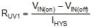
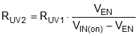
 Figure 8-1 Programmable Input Voltage UVLO
Turn-On
Figure 8-1 Programmable Input Voltage UVLO
Turn-On