ZHCSLO5B December 2020 – December 2021 LM25149
PRODUCTION DATA
- 1 特性
- 2 应用
- 3 说明
- 4 Revision History
- 5 说明(续)
- 6 Pin Configuration and Functions
- 7 Specifications
-
8 Detailed Description
- 8.1 Overview
- 8.2 Functional Block Diagram
- 8.3
Feature Description
- 8.3.1 Input Voltage Range (VIN)
- 8.3.2 High-Voltage Bias Supply Regulator (VCC, VCCX, VDDA)
- 8.3.3 Precision Enable (EN)
- 8.3.4 Power-Good Monitor (PG)
- 8.3.5 Switching Frequency (RT)
- 8.3.6 Active EMI Filter
- 8.3.7 Dual Random Spread Spectrum (DRSS)
- 8.3.8 Soft Start
- 8.3.9 Output Voltage Setpoint (FB)
- 8.3.10 Minimum Controllable On Time
- 8.3.11 Error Amplifier and PWM Comparator (FB, EXTCOMP)
- 8.3.12 Slope Compensation
- 8.3.13 Inductor Current Sense (ISNS+, VOUT)
- 8.3.14 Hiccup Mode Current Limiting
- 8.3.15 High-Side and Low-Side Gate Drivers (HO, LO)
- 8.3.16 Output Configurations (CNFG)
- 8.3.17 Single-Output Dual-Phase Operation
- 8.4 Device Functional Modes
-
9 Application and Implementation
- 9.1 Application Information
- 9.2
Typical Applications
- 9.2.1
Design 1 – High Efficiency 2.1-MHz Synchronous
Buck Regulator
- 9.2.1.1 Design Requirements
- 9.2.1.2
Detailed Design Procedure
- 9.2.1.2.1 Custom Design With WEBENCH® Tools
- 9.2.1.2.2 Custom Design With Excel Quickstart Tool
- 9.2.1.2.3 Buck Inductor
- 9.2.1.2.4 Current-Sense Resistance
- 9.2.1.2.5 Output Capacitors
- 9.2.1.2.6 Input Capacitors
- 9.2.1.2.7 Frequency Set Resistor
- 9.2.1.2.8 Feedback Resistors
- 9.2.1.2.9 Compensation Components
- 9.2.1.2.10 Active EMI Components
- 9.2.1.3 Application Curves
- 9.2.2 Design 2 – High Efficiency 440-kHz Synchronous Buck Regulator
- 9.2.3 Design 3 – Dual-Phase 400-kHz 20-A Synchronous Buck Regulator
- 9.2.1
Design 1 – High Efficiency 2.1-MHz Synchronous
Buck Regulator
- 10Power Supply Recommendations
- 11Layout
- 12Device and Documentation Support
- 13Mechanical, Packaging, and Orderable Information
8.3.9 Output Voltage Setpoint (FB)
The LM25149 output can be independently configured for one of three fixed output voltages without external feedback resistors, or adjusted to the desired voltage using an external resistor divider. Set the output to 3.3 V by connecting FB directly to VDDA. Alternatively, set the output to either 5 V or 12 V by installing a 24.9-kΩ or 49.9-kΩ resistor between FB and VDDA, respectively. See Table 8-1.
| PULLUP RESISTOR TO VDDA | VOUT SETPOINT |
|---|---|
| 0 Ω | 3.3 V |
| 24.9 kΩ | 5 V |
| 49.9 kΩ | 12 V |
| Not installed | External FB divider setting |
The configuration settings are latched and cannot be changed until the LM25149 is powered down (with the VCC voltage decreasing below its falling UVLO threshold) and then powered up again (VCC rises above 3.4-V typical). Alternatively, set the output voltage with an external resistive divider from the output to AGND. The output voltage adjustment range is between 0.8 V and 36 V. The regulation voltage at FB is 0.8 V (VREF). Use Equation 5 to calculate the upper and lower feedback resistors, designated as RFB1 and RFB2, respectively.
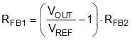
The recommended starting value for RFB2 is between 10 kΩ and 20 kΩ.
If low-IQ operation is required, take care when selecting the external feedback resistors. The current consumption of the external divider adds to the LM25149 sleep current (9.5-µA typical). The divider current reflected to VIN is scaled by the ratio of VOUT/VIN.