ZHCSLO5B December 2020 – December 2021 LM25149
PRODUCTION DATA
- 1 特性
- 2 应用
- 3 说明
- 4 Revision History
- 5 说明(续)
- 6 Pin Configuration and Functions
- 7 Specifications
-
8 Detailed Description
- 8.1 Overview
- 8.2 Functional Block Diagram
- 8.3
Feature Description
- 8.3.1 Input Voltage Range (VIN)
- 8.3.2 High-Voltage Bias Supply Regulator (VCC, VCCX, VDDA)
- 8.3.3 Precision Enable (EN)
- 8.3.4 Power-Good Monitor (PG)
- 8.3.5 Switching Frequency (RT)
- 8.3.6 Active EMI Filter
- 8.3.7 Dual Random Spread Spectrum (DRSS)
- 8.3.8 Soft Start
- 8.3.9 Output Voltage Setpoint (FB)
- 8.3.10 Minimum Controllable On Time
- 8.3.11 Error Amplifier and PWM Comparator (FB, EXTCOMP)
- 8.3.12 Slope Compensation
- 8.3.13 Inductor Current Sense (ISNS+, VOUT)
- 8.3.14 Hiccup Mode Current Limiting
- 8.3.15 High-Side and Low-Side Gate Drivers (HO, LO)
- 8.3.16 Output Configurations (CNFG)
- 8.3.17 Single-Output Dual-Phase Operation
- 8.4 Device Functional Modes
-
9 Application and Implementation
- 9.1 Application Information
- 9.2
Typical Applications
- 9.2.1
Design 1 – High Efficiency 2.1-MHz Synchronous
Buck Regulator
- 9.2.1.1 Design Requirements
- 9.2.1.2
Detailed Design Procedure
- 9.2.1.2.1 Custom Design With WEBENCH® Tools
- 9.2.1.2.2 Custom Design With Excel Quickstart Tool
- 9.2.1.2.3 Buck Inductor
- 9.2.1.2.4 Current-Sense Resistance
- 9.2.1.2.5 Output Capacitors
- 9.2.1.2.6 Input Capacitors
- 9.2.1.2.7 Frequency Set Resistor
- 9.2.1.2.8 Feedback Resistors
- 9.2.1.2.9 Compensation Components
- 9.2.1.2.10 Active EMI Components
- 9.2.1.3 Application Curves
- 9.2.2 Design 2 – High Efficiency 440-kHz Synchronous Buck Regulator
- 9.2.3 Design 3 – Dual-Phase 400-kHz 20-A Synchronous Buck Regulator
- 9.2.1
Design 1 – High Efficiency 2.1-MHz Synchronous
Buck Regulator
- 10Power Supply Recommendations
- 11Layout
- 12Device and Documentation Support
- 13Mechanical, Packaging, and Orderable Information
9.1.1.2 Output Capacitors
Ordinarily, the output capacitor energy storage of the regulator combined with the control loop response are prescribed to maintain the integrity of the output voltage within the dynamic (transient) tolerance specifications. The usual boundaries restricting the output capacitor in power management applications are driven by finite available PCB area, component footprint and profile, and cost. The capacitor parasitics—equivalent series resistance (ESR) and equivalent series inductance (ESL)—take greater precedence in shaping the load transient response of the regulator as the load step amplitude and slew rate increase.
The output capacitor, COUT, filters the inductor ripple current and provides a reservoir of charge for step-load transient events. Typically, ceramic capacitors provide extremely low ESR to reduce the output voltage ripple and noise spikes, while tantalum and electrolytic capacitors provide a large bulk capacitance in a relatively compact footprint for transient loading events.
Based on the static specification of peak-to-peak output voltage ripple denoted by ΔVOUT, choose an output capacitance that is larger than that given by Equation 14.
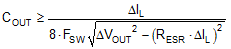
Figure 9-1 conceptually illustrates the relevant current waveforms during both load step-up and step-down transitions. As shown, the large-signal slew rate of the inductor current is limited as the inductor current ramps to match the new load-current level following a load transient. This slew-rate limiting exacerbates the deficit of charge in the output capacitor, which must be replenished as fast as possible during and after the load step-up transient. Similarly, during and after a load step-down transient, the slew rate limiting of the inductor current adds to the surplus of charge in the output capacitor that must be depleted as quickly as possible.
 Figure 9-1 Load Transient Response
Representation Showing COUT Charge Surplus or Deficit
Figure 9-1 Load Transient Response
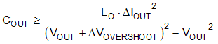
Representation Showing COUT Charge Surplus or DeficitIn a typical regulator application of 12-V input to low output voltage (for example, 3.3 V), the load-off transient represents the worst case in terms of output voltage transient deviation. In that conversion ratio application, the steady-state duty cycle is approximately 28% and the large-signal inductor current slew rate when the duty cycle collapses to zero is approximately –VOUT / L. Compared to a load-on transient, the inductor current takes much longer to transition to the required level. The surplus of charge in the output capacitor causes the output voltage to significantly overshoot. In fact, to deplete this excess charge from the output capacitor as quickly as possible, the inductor current must ramp below its nominal level following the load step. In this scenario, a large output capacitance can be advantageously employed to absorb the excess charge and minimize the voltage overshoot.
To meet the dynamic specification of output voltage overshoot during such a load-off transient (denoted as ΔVOVERSHOOT with step reduction in output current given by ΔIOUT), the output capacitance should be larger than:
The ESR of a capacitor is provided in the manufacturer’s data sheet either explicitly as a specification or implicitly in the impedance versus frequency curve. Depending on type, size, and construction, electrolytic capacitors have significant ESR, 5 mΩ and above, and relatively large ESL, 5 nH to 20 nH. PCB traces contribute some parasitic resistance and inductance as well. Ceramic output capacitors, on the other hand, have low ESR and ESL contributions at the switching frequency, and the capacitive impedance component dominates. However, depending on package and voltage rating of the ceramic capacitor, the effective capacitance can drop quite significantly with applied DC voltage and operating temperature.
Ignoring the ESR term in Equation 14 gives a quick estimation of the minimum ceramic capacitance necessary to meet the output ripple specification. Two to four 47-µF, 10-V, X7R capacitors in 1206 or 1210 footprint is a common choice for a 5-V output. Use Equation 15 to determine if additional capacitance is necessary to meet the load-off transient overshoot specification.
A composite implementation of ceramic and electrolytic capacitors highlights the rationale for paralleling capacitors of dissimilar chemistries yet complementary performance. The frequency response of each capacitor is accretive in that each capacitor provides desirable performance over a certain portion of the frequency range. While the ceramic provides excellent mid- and high-frequency decoupling characteristics with its low ESR and ESL to minimize the switching frequency output ripple, the electrolytic device with its large bulk capacitance provides low-frequency energy storage to cope with load transient demands.