ZHCSD41A DECEMBER 2012 – November 2014 LM10011
PRODUCTION DATA.
8 Application and Implementation
NOTE
Information in the following applications sections is not part of the TI component specification, and TI does not warrant its accuracy or completeness. TI’s customers are responsible for determining suitability of components for their purposes. Customers should validate and test their design implementation to confirm system functionality.
8.1 Application Information
LM10011 is a precision, digitally programmable device used for controlling the dc-dc converter output voltage. The LM10011 GUI design tool is available at www.ti.com/product/LM10011 and can be used to program any voltage regulator output to a desired range and resolution. The GUI enables changing the output voltage of the on-board POL based on direct user input. It is also able to assist the power designer in selecting the correct external components needed for any given application.
8.2 Typical Application
In this example, an LM21215A-1 is used as the voltage regulator and the desired range of output voltage operation is 0.7 V to 1.1 V. The LM10011 can provide control of the output voltage within this range with 6 bits or 4 bits of resolution. For this example, the 400 mV of voltage range translates to a VOUT_LSB of 400 mV / 63 = 6.4 mV (26.7 mV in 4-bit mode) at the regulator output. In this calculation, 1% resistor values are used. A schematic for this example is shown in Figure 12.
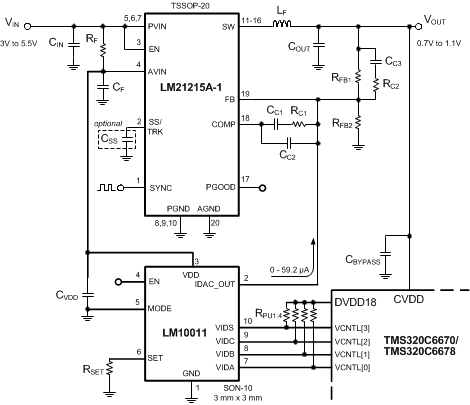 Figure 12. 6-Bit Mode Design Example
8.2.1 Design Requirements
Table 4 lists the design parameters.
Table 4. Design Parameters
| DESIGN PARAMETER | EXAMPLE VALUE |
|---|---|
| Output voltage range | 0.7 V to 1.1 V |
| Startup voltage | 1.1 V |
| Mode | 0 |
8.2.2 Detailed Design Procedure
8.2.2.1 Setting the VOUT Range and LSB
Looking at the Typical Application Circuit in Figure 12, the following equation defines VOUT of a given regulator (valid for VOUT > VFB):
Here, the output voltage is a function of the resistor divider from RFB1 and RFB2. Using the LM10011, there is a current supplied by the IDAC_OUT pin that helps drive current through the feedback resistor RFB2, thus lowering the necessary current supplied through RFB1, and hence lowering VOUT. To calculate the nominal (maximum) VOUT, use an IDAC_OUT value of 0 µA.
The change in the output voltage can be analyzed based on the resolution of the current DAC from the LM10011 compared to the desired resolution of the output swing of the regulator. RFB1 is designed to provide the desired VOUT_LSB with the equation:

Where LSB = LSB_6 (940 nA) from the electrical characteristics table (see Electrical Characteristics). Based on the desired nominal VOUT (with IDAC_OUT = 0 µA) and the calculated RFB1 from Equation 2, RFB2 can be solved using Equation 1.
8.2.2.2 4-Bit Mode Design Example
Designing with the LM10011 in 4-bit mode is similar to designing in 6-bit mode. The only differences are the LSB value (LSB = LSB_4 = 3.76 µA) in Equation 2 and full-scale current range (IDAC_OUT = 56.4 µA).
8.2.2.3 Setting the Start-Up Voltage with RSET
RSET is chosen depending on the required start-up voltage for the particular application. The user must use Equation 3 and solve for the required IDAC_OUT by inputting the known values of RFB1 and RFB2, VFB, and the desired start-up output voltage, VOUT. Once IDAC_OUT is solved for, choose an RSET based on Table 2 to select a start-up code to yield a current closely matching the calculated result. Use the equation below to solve for the required IDAC_OUT value at start-up.
8.2.2.4 Example Solution
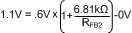
While in 6-bit mode, assuming a 400-mV output range, 64 VID codes, and an IDAC LSB of 0.940 µA, it is desired to have a VOUT with an LSB of 6.4 mV and a default value of 1.1 V with a 1.05-V start-up voltage using an LM21215A-1 regulator (VFB = 0.6 V):


Using 1% standard resistor values, RFB1 can be set to 6.81 kΩ. Now calculate RFB2 based on RFB1 and the maximum VOUT of 1.1 V using Equation 1.

Using 1% standard resistor values, RFB2 can be set to 8.06 kΩ. This will yield a regulator output range of 0.704 V (CODE 0d) to 1.107 V (CODE 63d). Values calculated here will be dependent on the accuracy of the regulator, the LM10011 IDAC_OUT, and the resistor values used in the circuit.
Table 5 shows the codes and some of the resultant values of the IDAC current and the corresponding regulator output voltage for the previous example.
Table 5. 6-Bit VID Codes with IDAC Current and Regulator Voltage for the Example in Figure 12.
| VID CODE | IDAC_OUT CURRENT (µA) | REGULATOR VOLTAGE (V) |
|---|---|---|
| 000000b (0d) | 59.2 | 0.704 |
| 000001b (1d) | 58.3 | 0.710 |
| 000010b (2d) | 57.4 | 0.716 |
| 000011b (3d) | 56.4 | 0.729 |
| .... | .... | .... |
| 111100b (60d) | 2.87 | 1.087 |
| 111101b (61d) | 1.93 | 1.094 |
| 111110b (62d) | 1.00 | 1.100 |
| 111111b (63d) | 0.06 | 1.107 |
The required IDAC_OUT value during start-up can be calculated based on the desired start-up voltage of 1.05 V and the RFB1 and RFB2 resistors found in the previous calculations. Using Equation 3 to solve for the required start-up IDAC_OUT current results in a start-up current of 8.36 µA.
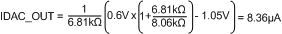
Choose a resistor in Table 2 that selects a start-up code that produces a current close to 8.36 µA. An RSET of 215 kΩ selects a nominal start-up code of 13d yielding a current of 7.59 µA and start-up voltage of 1.054 V.
NOTE
Using an RSET of 215 kΩ may also select a code of 14d (+1 LSB) yielding a current of 3.80 µA and a start-up voltage of 1.081 V.
8.2.3 Application Curves
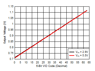 Figure 13. Output Voltage vs. Code for LM21k with LM10011