ZHCSD41A DECEMBER 2012 – November 2014 LM10011
PRODUCTION DATA.
7 Detailed Description
7.1 Overview
The LM10011 is a precision current DAC used for controlling any point of load regulator with an adjustable resistor feedback network. Four VID communication lines (VIDA, VIDB, VIDC, and VIDS) are used to write a 6-bit or 4-bit VID value. The output of the IDAC (IDAC_OUT) is used to inject a precision current into the feedback node of a regulator, thus adjusting the output voltage. With this method, it is possible to precisely control the output voltage of the regulator.
An enable pin (EN) is provided to allow for a reduced quiescent current when not in use. Also, the VDD line is monitored so that an undervoltage event will shutdown the LM10011 (IDAC_OUT = 0.0 µA).
The device is available in a 10-pad No-Pullback Package (SON-10). The LM10011 can be used in numerous applications with regulators from 2.97-V to 5.5-V supplies.
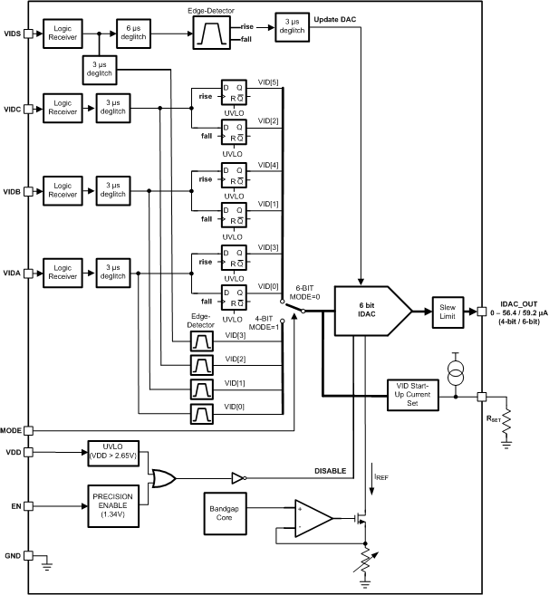
7.2 Functional Block Diagram
7.3 Feature Description
The LM10011 can be treated as a D/A converter, converting digital VID codes to analog outputs. The LM10011 DAC analog output is a current that flows out of the IDAC_OUT pin. The IDAC_OUT pin is intended to be connected to the feedback node of a voltage regulator as shown in Figure 11. In a typical voltage regulator, the current in RFB2 is constant by virtue of the regulator feedback loop maintaining the reference voltage at the feedback node. The current flowing through RFB2 is the same current flowing through RFB1. When current is injected into the feedback node by the LM10011, less current is required from the RFB1 resistor. The consequence of this is that the output voltage of the regulator will decrease to maintain the total amount of current in RFB2 to regulate at the correct feedback (reference) voltage.
Each VID code corresponds to a different IDAC_OUT current and thus a different output voltage. Increasing the VID code lowers the IDAC_OUT current and raises the output voltage. Decreasing the VID code raises the IDAC_OUT current and lowers the output voltage. All VID codes are decoded into a 6-bit or 4-bit current DAC output whether the MODE equals 0 (connected to GND) or 1 (connected to VDD), respectively.
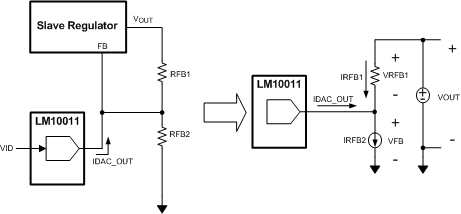 Figure 11. Output Voltage (VOUT) is Controlled Via Current Injection into the Feedback Node
7.3.1 Current DAC
The LM10011 current DAC is based on a low-voltage bandgap reference setting a current through a precision adjustable resistor. This bandgap is trimmed for precision and gives excellent performance over temperature. The output current has a maximum full-scale range [VID = 000000b] of 59.2 µA and is adjustable with a 6- or 4-bit VID word. This allows for 64 or 16 settings with a resolution of 940 nA or 3.76 µA, respectively. The current DAC also has a slew limit to prevent abrupt changes in the output. The slew limit is represented as a time constant, t6 = 40 µs, in the Electrical Characteristics table. A deglitch filter for the VID inputs provides noise immunity and effectively adds a small delay from the transition of a VID line to the change in IDAC_OUT current.
7.3.2 Enable Pin and UVLO
The enable (EN) pin allows the output of the device to be enabled or disabled (IDAC_OUT = 0.0 µA) with an external control signal. This pin is a precision analog input that enables the device when the voltage exceeds 1.34 V. The EN pin has 100 mV of hysteresis and will disable the output when the enable voltage falls below 1.23 V. If EN is not used, it can be left open, and will be pulled high by an internal 2-μA current source. Since the EN pin has a precise turn-on threshold it can be used along with an external resistor divider network from VDD to configure the device to turn on at a precise input voltage.
The LM10011 has a built-in undervoltage lockout (UVLO) protection circuit that keeps the device from operating until the input voltage reaches 2.65 V (typical). The UVLO threshold has 200 mV of hysteresis that keeps the LM10011 from responding to power-on glitches during start-up. Note that descending below the EN voltage and/or the UVLO voltage are functionally the same as a reset. Bringing the device back from a low enable setting or from a VDD UVLO event will reset the IDAC_OUT current to its start-up RSET setting.
7.4 Device Functional Modes
Table 1 lists the functional modes of the LM10011 device.
Table 1. Mode Pin Summary
| MODE PIN CONNECTION | LOGIC STATE | DESCRIPTION |
|---|---|---|
| GND | 0 | 6-bit mode |
| VDD | 1 | 4-bit mode |
7.5 Programming
7.5.1 VID Programming, 6-Bit Mode
Four pins are used to communicate with the LM10011. In 6-bit mode (MODE = 0), VIDA, VIDB, and VIDC are data lines, while VIDS is a latching strobe that programs in the LM10011 data. As shown in the 6-bit mode timing diagram of Figure 1, the falling edge of VIDS latches in the data from VIDA, VIDB, and VIDC as the lower three LSB of the IDAC_OUT value, [2:0]. After a minimum hold time (t2), the rising edge of VIDS latches in the data from VIDA, VIDB, and VIDC as the upper three LSB of the IDAC_OUT value, [5:3]. Internally, a delay (t3,t1) on VIDS allows for the setting of all VIDA, VIDB, and VIDC lines to change simultaneously as VIDS rises or falls.
7.5.2 VID Programming, 4-Bit Mode
The LM10011 includes a 4-bit mode to facilitate parallel VID communication. In 4-bit mode (MODE = 1), VIDC, VIDB, VIDA, and VIDS are all parallel data lines. As shown in the 4-bit mode timing diagram in Figure 1, a changing edge of any of the VID communication lines will change the IDAC_OUT current to the corresponding new 4-bit value found on the data lines. There is a 3-μs deglitch filter to eliminate spurious noise events. The data must overcome the deglitch time and the minimum hold time (t7) or else the IDAC_OUT pin current may not reflect the value indicated at the VID data inputs. During the hold time, no other data line can be transitioned.
As mentioned in a previous section, for both the 4-bit and 6-bit mode, the VID data word is set so that the lowest output current is seen at the highest VID data word (59.2 µA at a code of 0d in 6-bit mode and 56.4 µA in 4-bit mode). Conversely, the lowest current is seen at the highest VID data word (0.06 µA at 63d or 15d). During VID operation with the regulator, this will translate to the lowest output voltage with the lowest VID word, 0d, and the highest output voltage with the highest VID word, 63d or 15d. The communications pins can be used with a low-voltage microcontroller with a maximum VIL of 0.75 V and a minimum VIH of 1.0 V.
7.5.3 Programming the Start-Up Current
Depending on the value of RSET during start-up (when VDD > VUVLO_R and EN > VEN), the output current on the IDAC_OUT pin will take on 1 of 16 discrete values corresponding to the currents available in the 4-bit mode. These discrete start-up currents can be programmed by connecting a resistor (RSET) from the SET pin to GND. If the EN voltage is toggled or a UVLO is triggered during operation, the current will default back to the value set by the RSET resistor. It takes only one VID command transition in either 4-bit or 6-bit mode to change the current to something other than the pre-programmed start-up current. The required RSET resistors and their corresponding start-up currents codes can be found in Table 2.
Table 2. Start-Up–4-Bit Mode Currents with Corresponding RSET Values and Output Currents
| VID CODE | NOMINAL IDAC_OUT CURRENT (µA) | RSET (kΩ) |
|---|---|---|
| 0000b (0d) | 56.4 | 0 |
| 0001b (1d) | 52.7 | 21.0 |
| 0010b (2d) | 48.9 | 35.7 |
| 0011b (3d) | 45.2 | 51.1 |
| 0100b (4d) | 41.4 | 71.5 |
| 0101b (5d) | 37.7 | 86.6 |
| 0110b (6d) | 33.9 | 105 |
| 0111b (7d) | 30.1 | 118 |
| 1000b (8d) | 26.4 | 140 |
| 1001b (9d) | 22.6 | 154 |
| 1010b (10d) | 18.8 | 169 |
| 1011b (11d) | 15.1 | 182 |
| 1100b (12d) | 11.3 | 200 |
| 1101b (13d) | 7.59 | 215 |
| 1110b (14d) | 3.80 | 237 |
| 1111b (15d) | 0.06 | 301 |
Codes 0100b (4d) through 1110b (14d) will start-up into either the selected code or 1 code higher. This means that the output voltage of the POL may start-up into the selected output voltage or 1 LSB higher.
7.5.4 IDAC_OUT Current Values
Table 3. IDAC_OUT Currents and Corresponding VID Codes
| VID CODE (6-BIT [4-BIT]) | IDAC CURRENT (µA) |
|---|---|
| 0d | 59.2 |
| 1d | 58.3 |
| 2d | 57.4 |
| 3d [0d] | 56.4 |
| 4d | 55.5 |
| 5d | 54.6 |
| 6d | 53.6 |
| 7d [1d] | 52.7 |
| 8d | 51.7 |
| 9d | 50.8 |
| 10d | 49.8 |
| 11d [2d] | 48.9 |
| 12d | 48.0 |
| 13d | 47.0 |
| 14d | 46.1 |
| 15d [3d] | 45.2 |
| 16d | 44.2 |
| 17d | 43.3 |
| 18d | 42.3 |
| 19d [4d] | 41.4 |
| 20d | 40.5 |
| 21d | 39.5 |
| 22d | 38.6 |
| 23d [5d] | 37.7 |
| 24d | 36.7 |
| 25d | 35.7 |
| 26d | 34.8 |
| 27d [6d] | 33.9 |
| 28d | 33.0 |
| 29d | 32.0 |
| 30d | 31.1 |
| 31d [7d] | 30.1 |
| 32d | 29.2 |
| 33d | 28.2 |
| 34d | 27.3 |
| 35d [8d] | 26.4 |
| 36d | 25.4 |
| 37d | 24.5 |
| 38d | 23.6 |
| 39d [9d] | 22.6 |
| 40d | 21.6 |
| 41d | 20.7 |
| 42d | 19.8 |
| 43d [10d] | 18.8 |
| 44d | 17.9 |
| 45d | 17.0 |
| 46d | 16.0 |
| 47d [11d] | 15.1 |
| 48d | 14.1 |
| 49d | 13.2 |
| 50d | 12.3 |
| 51d [12d] | 11.3 |
| 52d | 10.4 |
| 53d | 9.50 |
| 54d | 8.52 |
| 55d [13d] | 7.59 |
| 56d | 6.60 |
| 57d | 5.70 |
| 58d | 4.74 |
| 59d [14d] | 3.80 |
| 60d | 2.87 |
| 61d | 1.93 |
| 62d | 1.00 |
| 63d [15d] | 0.06 |