ZHCSD41A DECEMBER 2012 – November 2014 LM10011
PRODUCTION DATA.
6 Specifications
6.1 Absolute Maximum Ratings(1)(2)
over operating free-air temperature range (unless otherwise noted)| MIN | MAX | UNIT | ||
|---|---|---|---|---|
| VDD, EN, IDAC_OUT, MODE | –0.3 | 6 | V | |
| VIDA, VIDB, VIDC, VIDS | –0.3 | 6 | V | |
| Junction Temperature | 150 | °C | ||
(1) Absolute Maximum Ratings indicate limits beyond which damage to the device may occur.
(2) If Military- or Aerospace-specified devices are required, please contact the Texas Instruments Sales Office / Distributors for availability and specifications.
6.2 Handling Ratings
| MIN | MAX | UNIT | |||
|---|---|---|---|---|---|
| Tstg | Storage temperature range | –65 | 150 | °C | |
| V(ESD) | Electrostatic discharge | Human body model (HBM), per ANSI/ESDA/JEDEC JS-001, all pins(1) | 2 | kV | |
| Charged device model (CDM), per JEDEC specification JESD22-C101, all pins(2) | 1 | ||||
(1) JEDEC document JEP155 states that 500-V HBM allows safe manufacturing with a standard ESD control process.
(2) JEDEC document JEP157 states that 250-V CDM allows safe manufacturing with a standard ESD control process.
6.3 Recommended Operating Conditions
over operating free-air temperature range (unless otherwise noted)| MIN | MAX | UNIT | ||
|---|---|---|---|---|
| VDD | 2.97 | 5.5 | V | |
| IDAC_OUT | –0.3 | VDD – 1.75 | V | |
| VIDA, VIDB, VIDC, VIDS, EN, MODE | –0.3 | 5.5 | V | |
| Junction Temperature | −40 | 125 | °C | |
| Ambient Temperature | −40 | 125 | °C | |
6.4 Thermal Information
| THERMAL METRIC(1) | LM10011 | UNIT | |
|---|---|---|---|
| DSC | |||
| 10 PINS | |||
| RθJA | Junction-to-ambient thermal resistance(2) | 52.1 | °C/W |
| RθJC(top) | Junction-to-case (top) thermal resistance(3) | 30.6 | |
| RθJB | Junction-to-board thermal resistance(4) | 26.8 | |
| ψJT | Junction-to-top characterization parameter(5) | 0.9 | |
| ψJB | Junction-to-board characterization parameter(6) | 26.9 | |
| RθJC(bot) | Junction-to-case (bottom) thermal resistance(7) | 7.7 | |
(1) For more information about traditional and new thermal metrics, see the IC Package Thermal Metrics application report, SPRA953.
(2) The junction-to-ambient thermal resistance under natural convection is obtained in a simulation on a JEDEC-standard, high-K board, as specified in JESD51-7, in an environment described in JESD51-2a.
(3) The junction-to-case (top) thermal resistance is obtained by simulating a cold plate test on the package top. No specific JEDEC-standard test exists, but a close description can be found in the ANSI SEMI standard G30-88.
(4) The junction-to-board thermal resistance is obtained by simulating in an environment with a ring cold plate fixture to control the PCB temperature, as described in JESD51-8.
(5) The junction-to-top characterization parameter, ψJT, estimates the junction temperature of a device in a real system and is extracted from the simulation data for obtaining RθJA, using a procedure described in JESD51-2a (sections 6 and 7).
(6) The junction-to-board characterization parameter, ψJB, estimates the junction temperature of a device in a real system and is extracted from the simulation data for obtaining RθJA, using a procedure described in JESD51-2a (sections 6 and 7).
(7) The junction-to-case (bottom) thermal resistance is obtained by simulating a cold plate test on the exposed (power) pad. No specific JEDEC standard test exists, but a close description can be found in the ANSI SEMI standard G30-88.
6.5 Electrical Characteristics
Typical values correspond to TJ = 25°C. Minimum and maximum limits apply over –40°C to 125°C junction temperature range unless otherwise stated.(4)(5)| PARAMETER | TEST CONDITIONS | MIN | TYP | MAX | UNIT | |
|---|---|---|---|---|---|---|
| SUPPLY, UVLO, AND ENABLE | ||||||
| IQ | Quiescent current | VDD = 5.0 V, VEN = 2.0 V | 260 | 300 | µA | |
| IQ_FS | Quiescent current, IDAC_OUT = IFS_6 | VDD = 5.0 V, VEN = 2.0 V, IFS_6 | 382 | µA | ||
| IQ_DIS | Quiescent current disabled | VDD = 5.0 V, VEN = 0.0 V | 45 | 65 | µA | |
| VUVLO_R | Undervoltage rising threshold | VDD rising | 2.65 | 2.95 | V | |
| VUVLO_F | Undervoltage falling threshold | VDD falling | 2.2 | 2.45 | V | |
| VUVLO_HYS | Hysteresis | 200 | mV | |||
| VEN | Enable rising threshold | VEN rising | 1.20 | 1.34 | 1.45 | V |
| VEN_HYS | Enable hysteresis | 50 | 100 | 180 | mV | |
| IEN | Enable pullup current | 2 | µA | |||
| IDAC_OUT | ||||||
| ACC | Accuracy | Measured at full scale | –1.25 | 1.25 | % | |
| ACC | Accuracy | Measured at full scale, 0°C to 100°C | –1.0 | 1.0 | % | |
| LSB_6 | DAC step size, 6-bit mode | IFS_6 / (26 – 1) | 940 | nA | ||
| LSB_4 | DAC step size, 4-bit mode | IFS_4 / (24 – 1) | 3.76 | µA | ||
| IFS_6 | Full-scale output current (6-bit mode) | VID[5:0] = 000000b | 59.2 | µA | ||
| IFS_4 | Full-scale output current (4-bit mode) | VID[3:0] = 0000b | 56.4 | µA | ||
| INL | Integral non-linearity | –1 | 1 | LSB_6 | ||
| DNL | Differential non-linearity | –0.25 | 0.25 | LSB_6 | ||
| OFFSET | Offset current | VID[5:0] = 111111b (6-bit), VID[3:0] = 1111b (4-bit) | 60 | nA | ||
| VOUT_MAX | IDAC_OUT compliance voltage | VDD = 3 V, VDD-VIDAC_OUT | 1.75 | V | ||
| START-UP SET CURRENT | ||||||
| VSETFSR | SET pin voltage FSR | 1.12 | 1.2 | 1.23 | V | |
| SETRES | SET ADC resolution | 4 | bits | |||
| SETRNG | SET ADC current full-scale range | 56.4 | µA | |||
| ISET | SET Current | 4.75 | 5.1 | 5.40 | µA | |
| SET0 | Start-up DAC error, code 0 | RSET = 0 Ω, IDAC_OUT = 56.4 µA | 0 | 0 | LSB | |
| SET1 | Start-up DAC error, code 1 | RSET = 21.0 kΩ(2), IDAC_OUT = 52.7 µA | 0 | 0 | LSB | |
| SET2 | Start-up DAC error, code 2 | RSET = 35.7 kΩ(2), IDAC_OUT = 48.9 µA | 0 | 0 | LSB | |
| SET3 | Start-up DAC error, code 3 | RSET = 51.1 kΩ(2), IDAC_OUT = 45.2 µA | 0 | 0 | LSB | |
| SET4 | Start-up DAC error, code 4(1) | RSET = 71.5 kΩ(2), IDAC_OUT = 41.4 µA | 0 | 1 | LSB | |
| SET5 | Start-up DAC error, code 5(1) | RSET = 86.6 kΩ(2), IDAC_OUT = 37.7 µA | 0 | 1 | LSB | |
| SET6 | Start-up DAC error, code 6(1) | RSET = 105 kΩ(2), IDAC_OUT = 33.9 µA | 0 | 1 | LSB | |
| SET7 | Start-up DAC error, code 7(1) | RSET = 118 kΩ(2), IDAC_OUT = 30.1 µA | 0 | 1 | LSB | |
| SET8 | Start-up DAC error, code 8(1) | RSET = 140 kΩ(2), IDAC_OUT =26.4 µA | 0 | 1 | LSB | |
| SET9 | Start-up DAC error, code 9(1) | RSET = 154 kΩ(2), IDAC_OUT = 22.6 µA | 0 | 1 | LSB | |
| SET10 | Start-up DAC error, code 10(1) | RSET = 169 kΩ(2), IDAC_OUT = 18.8 µA | 0 | 1 | LSB | |
| SET11 | Start-up DAC error, code 11(1) | RSET = 182 kΩ(2), IDAC_OUT = 15.1 µA | 0 | 1 | LSB | |
| SET12 | Start-up DAC error, code 12(1) | RSET = 200 kΩ(2), IDAC_OUT = 11.3 µA | 0 | 1 | LSB | |
| SET13 | Start-up DAC error, code 13(1) | RSET = 215 kΩ(2), IDAC_OUT = 7.59 µA | 0 | 1 | LSB | |
| SET14 | Start-up DAC error, code 14(1) | RSET = 237 kΩ(2), IDAC_OUT = 3.80 µA | 0 | 1 | LSB | |
| SET15 | Start-up DAC error, code 15 | RSET = 301 kΩ(2), IDAC_OUT = 0.06 µA | 0 | 0 | LSB | |
| VID LOGIC INPUTS(3) | ||||||
| VIL | Input voltage low | 0.75 | V | |||
| VIH | Input voltage high | 1.0 | V | |||
| IIL | Input current low | –3.5 | µA | |||
| IIH | Input current high | 5 | µA | |||
| tDEGLITCH | Input deglitch time | 3.6 | µs | |||
| t1 | Input delay time | VIDS rising edge | 1 | µs | ||
| t2 | Input hold time VIDA, VIDB, VIDC valid | VIDS falling edge | 20 | µs | ||
| t3 | Input delay time | VIDS falling edge | 1 | µs | ||
| t4 | Input hold time VIDA, VIDB, VIDC valid | VIDS rising edge | 20 | µs | ||
| t5 | Delay to beginning of IDAC_OUT transition | Measured from VIDS rising edge | 6.3 | 10 | µs | |
| t6 | IDAC_OUT transition time | Time constant for exponential rise | 40 | µs | ||
| t7 | Minimum hold time in 4-bit mode | VIDA, VIDB, VIDC, VIDS | 4.4 | µs | ||
(1) "+1" LSB implies a positive step in CODE. LSB is in reference to LSB_4.
(2) RSET is based on 1% E96 standard resistor values.
(3) For VID timing, see Figure 1.
(4) All hot and cold limits are specified by correlating the electrical characteristics to process and temperature variations and applying statistical process control.
(5) The junction temperature (TJ in °C) is calculated from the ambient temperature (TA in °C) and power dissipation (PD in Watts) as follows: TJ = TA + (PD × RθJA) where RθJA (in °C/W) is the package thermal impedance provided in the Thermal Information section.
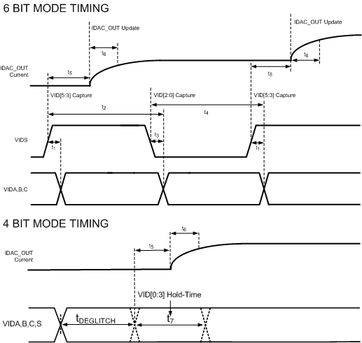 Figure 1. Timing Diagram for LM10011 Communications
6.6 Typical Characteristics
Unless otherwise specified, the following conditions apply: TJ = 25°C, VDD = 5 V. All graphs show junction temperature.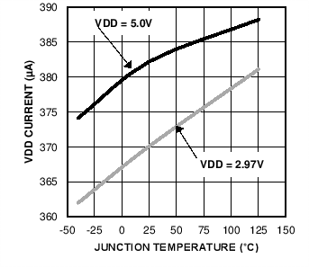 Figure 2. Supply Current
Maximum Output Current VID = [000000]
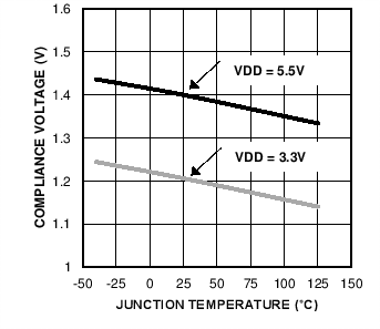 Figure 4. Output Compliance to Positive Rail
 (VDD-VIDAC_OUT)
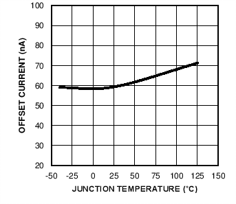 Figure 6. IDAC_OUT Offset Current
VID = [111111]
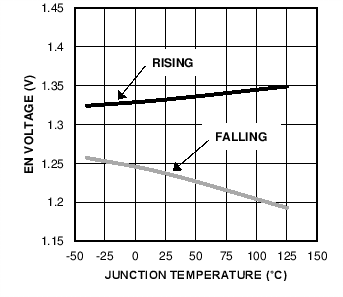 Figure 8. Enable (EN) Threshold
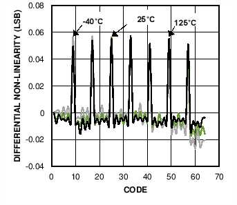 Figure 10. Differential Non-Linearity
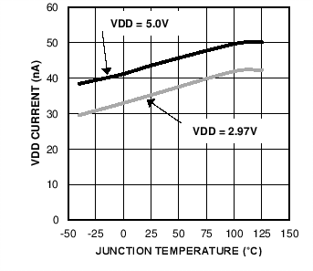 Figure 3. Supply Current (EN LOW)
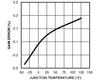 Figure 5. Gain Error
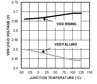 Figure 7. UVLO Thresholds
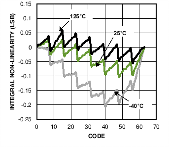 Figure 9. Integral Non-Linearity