ZHCSM23 December 2021 LDC3114
PRODUCTION DATA
- 1 特性
- 2 应用
- 3 说明
- 4 Revision History
- 5 Pin Configuration and Functions
- 6 Specifications
-
7 Detailed Description
- 7.1 Overview
- 7.2 Functional Block Diagram
- 7.3 Feature Description
- 7.4 Device Functional Modes
- 7.5 Register Maps
-
8 Application and Implementation
- 8.1
Application Information
- 8.1.1 Theory of Operation
- 8.1.2 Designing Sensor Parameters
- 8.1.3 Setting COM Pin Capacitor
- 8.1.4 Defining Power-On Timing
- 8.1.5 Configuring Button or Raw Data Scan Rate
- 8.1.6 Programming Button or Raw Data Sampling Window
- 8.1.7 Scaling Frequency Counter Output
- 8.1.8 Setting Button Triggering Threshold
- 8.1.9 Tracking Baseline
- 8.1.10 Mitigating False Button Detections
- 8.1.11 Reporting Interrupts for Button Presses, Raw Data Ready and Error Conditions
- 8.1.12 Estimating Supply Current
- 8.2 Typical Application
- 8.1
Application Information
- 9 Power Supply Recommendations
- 10Layout
- 11Device and Documentation Support
- 12Mechanical, Packaging, and Orderable Information
8.2.1 Touch Button Design
The low power architecture of LDC3114 makes them suitable for driving button sensors in consumer electronics, such as mobile phones. Most mobile phones today have three buttons along the edges, namely the power button, volume up, and volume down.
On a typical smartphone, the two volume buttons are next to each other, so they may be susceptible to false detections such as simultaneous button presses. To prevent such mis-triggers, they can be grouped together to take advantage of the various features that mitigate false detections as explained in Section 8.1.10. For example, if Max-win is applied to the two volume buttons, only the one with the greater force will be triggered.
The inductive touch solution does not require any mechanical cutouts at the button locations. This can support reduced manufacturing cost for the phone case and enhance the case resistance to moisture, dust, and dirt. This is a great advantage compared to mechanical buttons in the market today.
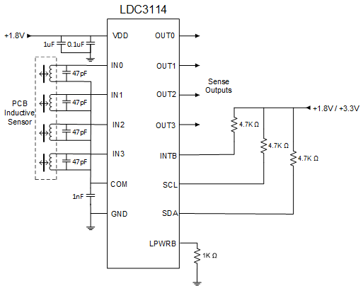
Figure 8-15 shows a typical touch button application.

Figure 8-15 Application Schematic