ZHCSCB1 March 2014 LDC1041
PRODUCTION DATA.
- 1 特性
- 2 应用范围
- 3 说明
- 4 修订历史记录
- 5 Terminal Configuration and Functions
- 6 Specifications
- 7 Detailed Description
- 8 Applications and Implementation
- 9 Power Supply Recommendations
- 10Layout
- 11器件和文档支持
- 12机械封装和可订购信息
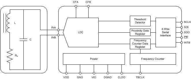
7 Detailed Description
7.1 Overview
The LDC1041 is an Inductance-to-Digital Converter that simultaneously measures the impedance and resonant frequency of an LC resonator. It accomplishes this task by regulating the oscillation amplitude in a closed loop configuration to a constant level, while monitoring the energy dissipated by the resonator. By monitoring the amount of power injected into the resonator, the LDC1041 can determine the value of Rp; it returns this as a digital value which is inversely proportional to Rp. In addition, the LDC1041 also measure the oscillation frequency of the LC circuit; this frequency is used to determine the inductance of the LC circuit. The device outputs a digital value that is inversely proportional to frequency.
The threshold detector block provides a comparator with hysteresis, with the threshold registers programed and comparator enabled, proximity data register is compared with threshold registers and INTB pin indicates the output.
The device has a simple 4-wire SPI interface. The INTB pin provides multiple functions which are programmable with SPI.
The device has separate supplies for Analog and I/O, with analog operating at 5V and I/O at 1.8-5V. The integrated LDO needs a 56nF capacitor connected from CLDO pin to GND.
7.2 Functional Block Diagram
7.3 Feature Description
7.3.1 Inductive Sensing
An AC current flowing through a coil will generate an AC magnetic field. If a conductive material, such as a metal target, is brought into the vicinity of the coil, this magnetic field will induce circulating currents (eddy currents) on the surface of the target. These eddy currents are a function of the distance, size, and composition of the target. The eddy currents then generate their own magnetic field, which opposes the original field generated by the coil. This mechanism is best compared to a transformer, where the coil is the primary core and the eddy current is the secondary core. The inductive coupling between both cores depends on distance and shape. Hence the resistance and inductance of the secondary core (eddy current), shows up as a distant dependent resistive and inductive component on the primary side (coil). Figure 5 to Figure 8 show a simplified circuit model.
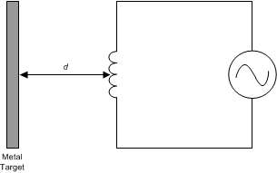 Figure 5. Inductor With A Metal Target
Eddy currents generated on the surface of the target can be modeled as a transformer as shown in Figure 6. The coupling between the primary and secondary coils is a function of the distance and the conductor’s characteristics. In Figure 6, the inductance Ls is the coil’s inductance, and Rs is the coil’s parasitic series resistance. The inductance L(d), which is a function of distance d, is the coupled inductance of the metal target. Likewise, R(d) is the parasitic resistance of the eddy currents and is also a function of distance.
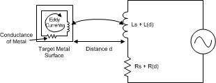 Figure 6. Metal Target Modeled As L And R With Circulating Eddy Currents
Generating an alternating magnetic field with just an inductor will consume a large amount of power. This power consumption can be reduced by adding a parallel capacitor, turning it into a resonator as shown in Figure 7 . In this manner the power consumption is reduced to the eddy and inductor losses Rs+R(d) only.
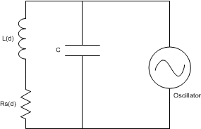 Figure 7. LC Tank Connected To Oscillator
The LDC1041 doesn’t measure the series resistance directly; instead it measures the equivalent parallel resonance impedance Rp (see Figure 8). This representation is equivalent to the one shown in Figure 8 , where the parallel resonance impedance Rp(d) is given by:
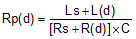
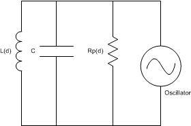 Figure 8. Equivalent Resistance Of Rs in Parallel With LC Tank
Figure 9 below shows the variation in Rp as a function of distance for a 14mm diameter PCB coil (Sensor Details:Table 19). The target in this example is a section of a 2mm thick stainless steel disk.
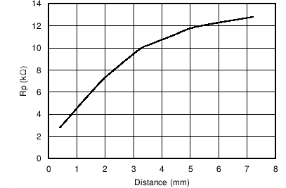 Figure 9. Typical Rp vs Distance With 14mm PCB Coil
7.3.2 Measuring Rp with LDC1041
The LDC1041 supports a wide range of LC combinations, with oscillation frequencies ranging from 5kHz to 5MHz and Rp ranging from 798Ω to 3.93MΩ. This range of Rp can be viewed as the maximum input range of an ADC. As illustrated in Figure 9, the range of Rp is typically much smaller than the maximum input range supported by the LDC1041. To get better resolution in the desired sensing range, the LDC1041 offers a programmable input range through the Rp_MIN and Rp_MAX registers. Refer to Calculation of Rp_MIN and Rp_MAX below for how to set these registers.
When the sensor’s resonance impedance Rp drops below the programed Rp_MIN, the LDC’s Rp output will clip at its full scale output. This situation could, for example, happen when a target comes too close to the coil.
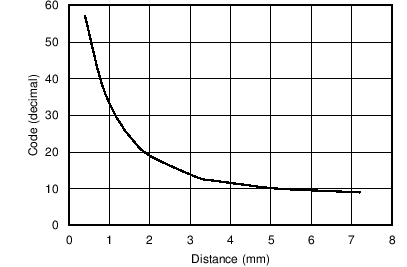 Figure 10. Transfer Characteristics Of LDC1041 With Rp_MIN= 1.347 kΩ And Rp_MAX= 38.785 kΩ
The resonance impedance can be calculated from the digital output code as follows:
where
- Y=Proximity Data/27
- Rp_MAX and Rp_MIN are the maximum and minimum Rp values selected in the respective registers
- Proximity data is the LDC output, register address 0x22.
Example: If Proximity data (address 0x22) is 50, Rp_MIN is 2.394 kΩ, and Rp_MAX is 38.785 kΩ, the resonance impedance is given by:
Y=50/27 = 0.3906
Rp=(38785*2394)/(2394×(1-0.3906) + 38785×0.3906) =(92851290)/(15149.421 + 1458.9036)
Rp = 5.59 kΩ
7.3.3 Measuring Inductance with LDC1041
LDC1041 measures the sensor’s frequency of oscillation using a frequency counter. The frequency counter timing is set by an external clock applied on TBCLK terminal. The sensor frequency can be calculated from the frequency counter register value (see registers 0x23 through 0x25) as follows:

where
- Fext is the frequency of the external clock
- Fcount is the value obtained from the Frequency Counter Data register(address 0x23,0x24,0x25)
- Response Time is the programmed response time (see LDC configuration register, address 0x04)
The sensor inductance can be determined by:
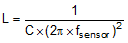
where
- C is the parallel capacitance of the resonator
Example: If Fext=6MHz, Response time=6144, C=100pF and measured Fcount= 3000 (dec) (address 0x23 through 0x25)
fsensor=(1/3)*(6000000/3000)*(6144)= 4.096MHz
Now using,
Inductance, L = 15.098 µH
The accuracy of measurement largely depends upon the choice of the external time-base clock (TBCLK). A higher frequency will provide better measurement accuracy.
7.4 Device Functional Modes
7.4.1 Power Modes
The LDC1041 has two power modes:
- Active Mode : In this mode the Proximity data and frequency data conversion is enabled.
- Stand-by Mode: This is the default mode on device power-up. In this mode conversion is disabled.
7.4.2 INTB Pin Modes
The INTB terminal is a configurable output terminal which can be used to drive an interrupt on an MCU. The LDC1041 provides three different modes on INTB terminal:
- Comparator Mode
- Wake-Up Mode
- DRDY Mode
LDC1041 has built-in High and Low trigger threshold registers which can be used as a comparator with programmable hysteresis or in a special mode which can be used to wake-up an MCU. These modes are explained in detail below.
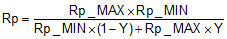
7.4.2.1 Comparator Mode
In the Comparator mode, the INTB terminal is asserted or deasserted when the proximity register value increases above Threshold High or decreases below Threshold Low registers respectively. In this mode, the LDC1041 essentially behaves as a proximity switch with programmable hysteresis.
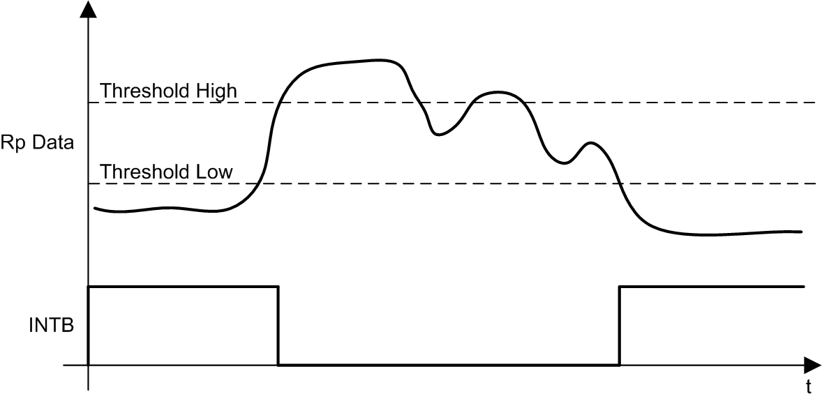 Figure 11. Behavior Of INTB Terminal In Comparator Mode
7.4.2.2 Wake-Up Mode
In Wake-Up mode, the INTB terminal is asserted when proximity register value increases above Threshold High and de-asserted when wake-up mode is disabled in INTB terminal mode register.
This mode can be used to wake-up an MCU from sleep, to conserve power.
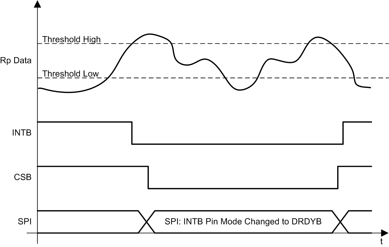 Figure 12. Behavior Of INTB Terminal In Wake-Up Mode
7.4.2.3 DRDYB Mode
In DRDY(Data Ready) mode, the INTB terminal is asserted every time the conversion data is available and de-asserted once the read command on register 0x22 is registered internally; if the read is in progress, the terminal is pulsed instead. The valid condition for new data availability is CSB high and DRDYB falling edge.
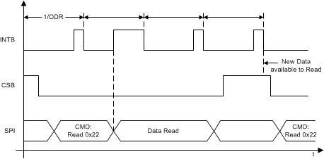 Figure 13. Behavior of INTB Terminal in DRDYB Mode with SPI Extending Beyond Subsequent Conversions
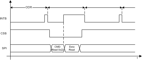 Figure 14. Behavior Of INTB Terminal In DRDYB Mode with SPI Reading The Data Within Subsequent Conversion
7.5 Programming
The LDC1041 utilizes a 4-wire SPI to access control and data registers. The LDC1041 is an SPI slave device and does not initiate any transactions.
7.5.1 SPI Description
A typical serial interface transaction begins with an 8-bit instruction, which is comprised of a read/write bit (MSB, R=1) and a 7 bit address of the register, followed by a data field which is typically 8 bits. However, the data field can be extended to a multiple of 8 bits by providing sufficient SPI clocks. Refer to the Extended SPI Transactions section below.
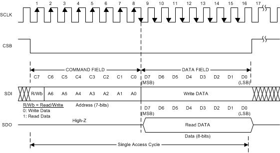 Figure 15. Serial Interface Protocol
Each assertion of CSB starts a new register access. The R/Wb bit in the command field configures the direction of the access; a value of 0 indicates a write operation and a value of 1 indicates a read operation. All output data is driven on the falling edge of the serial clock (SCLK), and all input data is sampled on the rising edge of the serial clock (SCLK). Data is written into the register on the rising edge of the 16th clock. It is required to deassert CSB after the 16th clock; if CSB is deasserted before the 16th clock, no data write will occur.
7.5.1.1 Extended SPI Transactions
A transaction may be extended to multiple registers by keeping the CSB asserted beyond the initial 16 clocks. In this mode, the register addresses increment automatically. CSB must be asserted during 8*(1+N) clock cycles of SCLK, where N is the amount of bytes to write or read during the transaction.
During an extended read access, SDO outputs the register contents every 8 clock cycles after the initial 8 clocks of the command field. During an extended write access, the data is written to the registers every 8 clock cycles after the initial 8 clocks of the command field.
Extended transactions can be used to read 8-bits of Proximity data and 24-bits of frequency data in a single SPI transaction by initiating a read from the register 0x22.
7.6 Register Map and Description
Table 1. Register Map(1)(2)(3)
| Register Name | Address | Direction | Default | Bit 7 | Bit 6 | Bit 5 | Bit 4 | Bit 3 | Bit 2 | Bit 1 | Bit 0 |
|---|---|---|---|---|---|---|---|---|---|---|---|
| Device ID | 0x00 | RO | 0x84 | Device ID | |||||||
| Rp_MAX | 0x01 | R/W | 0x0E | Rp Maximum | |||||||
| Rp_MIN | 0x02 | R/W | 0x14 | Rp Minimum | |||||||
| Watchdog Timer Frequency | 0x03 | R/W | 0x45 | Min Sensor Frequency | |||||||
| LDC Configuration | 0x04 | R/W | 0x1B | Reserved(000) | Amplitude | Response Time | |||||
| Reserved | 0x05 | RO | 0x01 | Reserved(00000001) | |||||||
| Reserved | 0x06 | R/W | 0xFF | Reserved | |||||||
| Comparator Threshold High MSB | 0x07 | R/W | 0xFF | Threshold High MSB | |||||||
| Reserved | 0x08 | R/W | 0x00 | Reserved | |||||||
| Comparator Threshold Low MSB | 0x09 | R/W | 0x00 | Threshold Low MSB | |||||||
| INTB Terminal Configuration | 0x0A | R/W | 0x00 | Reserved(00000) | INTB_MODE | ||||||
| Power Configuration | 0x0B | R/W | 0x00 | Reserved(0000000) | PWR_MODE | ||||||
| Status | 0x20 | RO | OSC Dead | DRDYB | Wake-up | Comparator | Do Not Care | ||||
| Reserved | 0x21 | RO | Reserved(00000000) | ||||||||
| Proximity Data | 0x22 | RO | Proximity Data | ||||||||
| Frequency Counter Data LSB | 0x23 | RO | FCOUNT LSB | ||||||||
| Frequency Counter Data Mid-Byte | 0x24 | RO | FCOUNT Mid Byte | ||||||||
| Frequency Counter Data MSB | 0x25 | RO | FCOUNT MSB | ||||||||
Table 2. Revision ID
| Address = 0x00, Default=0x84, Direction=RO | ||
|---|---|---|
| Bit Field | Field Name | Description |
| 7:0 | Revision ID | Revision ID of Silicon. |
Table 3. Rp_MAX
| Address = 0x01, Default=0x0E, Direction=R/W | ||
|---|---|---|
| Bit Field | Field Name | Description |
| 7:0 | Rp Maximum | Maximum Rp that LDC1041 needs to measure. Configures the input dynamic range of LDC1041. See Table 4 for register settings. |
Table 4. Register Settings for Rp_MAX
| Register setting | Rp (kΩ) |
|---|---|
| 0x00 | 3926.991 |
| 0x01 | 3141.593 |
| 0x02 | 2243.995 |
| 0x03 | 1745.329 |
| 0x04 | 1308.997 |
| 0x05 | 981.748 |
| 0x06 | 747.998 |
| 0x07 | 581.776 |
| 0x08 | 436.332 |
| 0x09 | 349.066 |
| 0x0A | 249.333 |
| 0x0B | 193.926 |
| 0x0C | 145.444 |
| 0x0D | 109.083 |
| 0x0E | 83.111 |
| 0x0F | 64.642 |
| 0x10 | 48.481 |
| 0x11 | 38.785 |
| 0x12 | 27.704 |
| 0x13 | 21.547 |
| 0x14 | 16.160 |
| 0x15 | 12.120 |
| 0x16 | 9.235 |
| 0x17 | 7.182 |
| 0x18 | 5.387 |
| 0x19 | 4.309 |
| 0x1A | 3.078 |
| 0x1B | 2.394 |
| 0x1C | 1.796 |
| 0x1D | 1.347 |
| 0x1E | 1.026 |
| 0x1F | 0.798 |
Table 5. Rp_MIN
| Address = 0x02, Default=0x14, Direction=R/W | ||
|---|---|---|
| Bit Field | Field Name | Description |
| 7:0 | Rp Minimum | Minimum Rp that LDC1041 needs to measure. Configures the input dynamic range of LDC1041. See Table 6 for register settings.(1) |
Table 6. Register Settings for Rp_MIN
| Register setting | Rp (kΩ) |
|---|---|
| 0x20 | 3926.991 |
| 0x21 | 3141.593 |
| 0x22 | 2243.995 |
| 0x23 | 1745.329 |
| 0x24 | 1308.997 |
| 0x25 | 981.748 |
| 0x26 | 747.998 |
| 0x27 | 581.776 |
| 0x28 | 436.332 |
| 0x29 | 349.066 |
| 0x2A | 249.333 |
| 0x2B | 193.926 |
| 0x2C | 145.444 |
| 0x2D | 109.083 |
| 0x2E | 83.111 |
| 0x2F | 64.642 |
| 0x30 | 48.481 |
| 0x31 | 38.785 |
| 0x32 | 27.704 |
| 0x33 | 21.547 |
| 0x34 | 16.160 |
| 0x35 | 12.120 |
| 0x36 | 9.235 |
| 0x37 | 7.182 |
| 0x38 | 5.387 |
| 0x39 | 4.309 |
| 0x3A | 3.078 |
| 0x3B | 2.394 |
| 0x3C | 1.796 |
| 0x3D | 1.347 |
| 0x3E | 1.026 |
| 0x3F | 0.798 |
Table 7. Watchdog Timer Frequency
| Address = 0x03, Default=0x45, Direction=R/W | ||
|---|---|---|
| Bit Field | Field Name | Description |
| 7:0 | Min Sensor Frequency | Sets the watchdog timer. The Watchdog timer is set based on the lowest sensor frequency. Equation 5. Example: where
If Sensor frequency is 1Mhz Min Sensor Frequency=68.94*log10(1M/2500)=Round to nearest integer(179.38)=179 |
Table 8. LDC Configuration
| Address = 0x04, Default=0x1B, Direction=R/W | ||
|---|---|---|
| Bit Field | Field Name | Description |
| 7:5 | Reserved | Reserved to 0 |
| 4:3 | Amplitude | Sets the oscillation amplitude |
| 00:1V | ||
| 01:2V | ||
| 10:4V | ||
| 11:Reserved | ||
| 2:0 | Response Time | 000: Reserved |
| 001: Reserved | ||
| 010: 192 | ||
| 011: 384 | ||
| 100: 768 | ||
| 101: 1536 | ||
| 110: 3072 | ||
| 111: 6144 | ||
Table 9. Comparator Threshold High MSB
| Address = 0x07, Default=0xFF, Direction=R/W | ||
|---|---|---|
| Bit Field | Field Name | Description |
| 7:0 | Threshold High | Threshold High Register. |
Table 10. Comparator Threshold Low MSB
| Address = 0x09, Default=0x00, Direction=R/W | ||
|---|---|---|
| Bit Field | Field Name | Description |
| 7:0 | Threshold Low | Threshold Low Register. |
Table 11. INTB Terminal Configuration
| Address = 0x0A, Default=0x00, Direction=R/W | ||
|---|---|---|
| Bit Field | Field Name | Description |
| 7:3 | Reserved | Reserved to 0 |
| 2:0 | Mode | 000: All modes disabled |
| 001: Wake-up Enabled on INTB terminal | ||
| 010: INTB terminal indicates the status of Comparator output | ||
| 100: DRDYB Enabled on INTB terminal | ||
| All other combinations are Reserved | ||
Table 12. Power Configuration
| Address = 0x0B, Default=0x00, Direction=R/W | ||
|---|---|---|
| Bit Field | Field Name | Description |
| 7:1 | Reserved | Reserved to 0 |
| 0 | PWR_MODE | 0:Stand-By mode
1:Active Mode. Conversion is Enabled Refer to Power Modes for more details. |
Table 13. Status
| Address = 0x20, Default=NA, Direction=RO | ||
|---|---|---|
| Bit Field | Field Name | Description |
| 7 | OSC status | 1:Indicates oscillator overloaded and stopped |
| 0:Oscillator working | ||
| 6 | Data Ready | 1:No new data available |
| 0:Data is ready to be read | ||
| 5 | Wake-up | 1:Wake-up disabled |
| 0:Wake-up triggered. Proximity data is more than Threshold High value. | ||
| 4 | Comparator | 1:Proximity data is less than Threshold Low value |
| 0:Proximity data is more than Threshold High value | ||
| 3:0 | Do not Care | |
Table 14. Proximity Data
| Address = 0x22, Default=NA, Direction=RO | ||
|---|---|---|
| Bit Field | Field Name | Description |
| 7:0 | Proximity data | Proximity data |
Table 15. Frequency Counter LSB
| Address = 0x23, Default=NA, Direction=RO | ||
|---|---|---|
| Bit Field | Field Name | Description |
| 7:0 | FCOUNT LSB (FCOUNT[7:0]) | LSB of Frequency Counter. Sensor frequency can be calculated using the output data rate. Please refer to the Measuring Inductance with LDC1041. |
Table 16. Frequency Counter Mid-Byte
| Address = 0x24, Default=NA, Direction=RO | ||
|---|---|---|
| Bit Field | Field Name | Description |
| 7:0 | FCOUNT Mid byte (FCOUNT[15:8]) | Middle Byte of Output data rate |
Table 17. Frequency Counter MSB
| Address = 0x25, Default=NA, Direction=RO | ||
|---|---|---|
| Bit Field | Field Name | Description |
| 7:0 | FCOUNT MSB (FCOUNT[23:16]) | MSB of Output data rate |
Conversion data is updated to these registers only when a read is initiated on 0x22 register. If the read is delayed between subsequent conversions, these registers are not updated until another read is initiated on 0x22.