ZHCSCB1 March 2014 LDC1041
PRODUCTION DATA.
- 1 特性
- 2 应用范围
- 3 说明
- 4 修订历史记录
- 5 Terminal Configuration and Functions
- 6 Specifications
- 7 Detailed Description
- 8 Applications and Implementation
- 9 Power Supply Recommendations
- 10Layout
- 11器件和文档支持
- 12机械封装和可订购信息
6 Specifications
6.1 Absolute Maximum Ratings(1)
| MIN | MAX | UNIT | ||
|---|---|---|---|---|
| Analog Supply Voltage (VDD – GND) | 6 | V | ||
| IO Supply Voltage (VIO – GND) | 6 | V | ||
| Voltage on any Analog Terminal | –0.3 | VDD + 0.3 | V | |
| Voltage on any Digital Terminal | –0.3 | VIO + 0.3 | V | |
| Input Current on INA and INB | 8 | mA | ||
| Junction Temperature, TJ(2) | 150 | °C | ||
(1) Absolute Maximum Ratings are limits beyond which damage to the device may occur. Exposure to absolute-maximum-rated conditions for extended periods may affect device reliability. Operating Ratings are conditions under which operation of the device is intended to be functional. For ensured specifications and test conditions, see the Electrical Characteristics.
(2) The maximum power dissipation is a function of TJ(MAX), θJA, and the ambient temperature, TA. The maximum allowable power dissipation at any ambient temperature is PDMAX = (TJ(MAX) - TA)/ θJA. All numbers apply for packages soldered directly onto a PC board. The package thermal impedance is calculated in accordance with JESD 51-7.
6.2 Handling Ratings
| MIN | MAX | UNIT | ||
|---|---|---|---|---|
| Tstg | Storage Temperature Range | -65 | 150 | °C |
| VESD(1) | Human Body Model (HBM) ESD stress voltage (2) | 1k | 1k | V |
| Charge Device Model (CDM) ESD stress voltage(3) | 250 | 250 | V |
(1) Electrostatic discharge (ESD) to measure device sensitivity and immunity to damage caused by assembly line electrostatic discharges in to the device.
(2) Level listed above is the passing level per ANSI, ESDA, and JEDEC JS-001. JEDEC document JEP155 states that 500-V HBM allows safe manufacturing with a standard ESD control process.
(3) Level listed above is the passing level per EIA-JEDEC JESD22-C101. JEDEC document JEP157 states that 250-V CDM allows safe manufacturing with a standard ESD control process.
6.3 Recommended Operating Conditions(1)
over operating free-air temperature range (unless otherwise noted)| MIN | MAX | UNIT | ||
|---|---|---|---|---|
| Analog Supply Voltage (VDD – GND) | 4.75 | 5.25 | V | |
| IO Supply Voltage (VIO – GND) | 1.8 | 5.25 | V | |
| VDD-VIO | 0 | V | ||
| Operating Temperature, TA | -40 | 125 | °C | |
6.4 Thermal Information
| THERMAL METRIC(1) | NHR (16-TERMINALS) |
UNIT | |
|---|---|---|---|
| θJA | Junction-to-ambient thermal resistance | 28 | °C/W |
(1) For more information about traditional and new thermal metrics, see the IC Package Thermal Metrics application report, SPRA953.
6.5 Electrical Characteristics(1)
Unless otherwise specified, all limits ensured for TA = TJ = 25°C, VDD = 5 V, VIO = 3.3 V(2)| PARAMETER | TEST CONDITIONS | MIN(3) | TYP(2) | MAX(3) | UNIT | |
|---|---|---|---|---|---|---|
| POWER | ||||||
| VDD | Analog supply voltage | 4.75 | 5 | 5.25 | V | |
| VIO | IO supply voltage | VIO≤VDD | 1.8 | 3.3 | 5.25 | V |
| IDD | Supply current, VDD | Does not include sensor current.(4) | 1.7 | 2.3 | mA | |
| IVIO | IO supply current | Static current | 14 | µA | ||
| IDD_LP | Stand-by mode supply current | 250 | µA | |||
| tSTART | Start-Up Time | From POR to ready-to-convert. | 2 | ms | ||
| LDC | ||||||
| ƒsensor_MIN | Minimum sensor frequency | 5 | kHz | |||
| ƒsensor_MAX | Maximum sensor frequency | 5 | MHz | |||
| Asensor_MIN | Minimum sensor amplitude | 1 | VPP | |||
| Asensor_MAX | Maximum sensor amplitude | 4 | VPP | |||
| tREC | Recovery time | Oscillation start-up time after Rp under-range condition | 10 | 1/fsensor | ||
| Rp Min | Minimum sensor Rp range | 798 | Ω | |||
| Rp Max | Maximum Sensor Rp range | 3.93 | MΩ | |||
| Rp Res | Rp measurement resolution | 8 | Bits | |||
| L Res | Inductance measurement resolution | 24 | Bits | |||
| tS_MIN | Minimum response time | Minimum programmable settling time of digital filter | 192 × 1 / ƒsensor | s | ||
| tS_MAX | Maximum response time | Maximum programmable settling time of digital filter | 6144 × 1 / ƒsensor | s | ||
| EXTERNAL CLOCK | ||||||
| ƒ | External clock frequency | 8 | MHz | |||
| DIGITAL I/O CHARACTERISTICS | ||||||
| VIH | Logic 1 input voltage | 0.8 × VIO | V | |||
| VIL | Logic 0 input voltage | 0.2 × VIO | V | |||
| VOH | Logic 1 output voltage | ISOURCE = 400 µA | VIO – 0.3 | V | ||
| VOL | Logic 0 output voltage | ISINK = 400 µA | 0.3 | V | ||
| IIOHL | Digital IO leakage current | –500 | 500 | nA | ||
(1) Electrical Characteristics Table values apply only for factory testing conditions at the temperature indicated. Factory testing conditions result in very limited self-heating of the device such that TJ = TA. No specification of parametric performance is indicated in the electrical tables under conditions of internal self-heating where TJ > TA. Absolute Maximum Ratings indicate junction temperature limits beyond which the device may be permanently degraded, either mechanically or electrically.
(2) Typical values represent the most likely parametric norm as determined at the time of characterization. Actual typical values may vary over time and will also depend on the application and configuration. The typical values are not tested and are not specified on shipped production material.
(3) Limits are specified by testing, design, or statistical analysis at 25°C. Limits over the operating temperature range are specified through correlations using statistical quality control (SQC) method.
(4) LC tank current depends on the Q-factor of the tank, distance and material of the target.
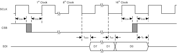
6.6 Timing Requirements
Unless otherwise noted, all limits specified at TA = 25°C, VDD = 5, VIO = 3.3, 10 pF capacitive load in parallel with a 10 kΩ load on the SDO terminal. Specified by design; not production tested.| PARAMETER | MIN | TYP | MAX | UNIT | ||
|---|---|---|---|---|---|---|
| ƒSCLK | Serial Clock Frequency | 4 | MHz | |||
| tPH | SCLK Pulse Width High | ƒSCLK = 4 MHz | 0.4 / ƒSCLK | s | ||
| tPL | SCLK Pulse Width Low | ƒSCLK = 4 MHz | 0.4 / ƒSCLK | s | ||
| tSU | SDI Setup Time | 10 | ns | |||
| tH | SDI Hold Time | 10 | ns | |||
| tODZ | SDO Driven-to-Tristate Time | Measured at 10% / 90% point | 20 | ns | ||
| tOZD | SDO Tristate-to-Driven Time | Measured at 10% / 90% point | 20 | ns | ||
| tOD | SDO Output Delay Time | 20 | ns | |||
| tCSS | CSB Setup Time | 20 | ns | |||
| tCSH | CSB Hold Time | 20 | ns | |||
| tIAG | Inter-Access Gap | 100 | ns | |||
| tDRDYB | Data ready pulse width | Data ready pulse at every 1 / ODR if no data is read | 1 / ƒsensor | s | ||
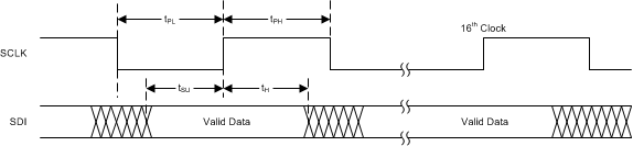 Figure 1. Write Timing Diagram