ZHCSLE0B August 2021 – August 2023 JFE2140
PRODUCTION DATA
- 1
- 1 特性
- 2 应用
- 3 说明
- 4 Revision History
- 5 Pin Configuration and Functions
- 6 Specifications
- 7 Parameter Measurement Information
- 8 Detailed Description
- 9 Application and Implementation
- 10Device and Documentation Support
- 11Mechanical, Packaging, and Orderable Information
封装选项
机械数据 (封装 | 引脚)
散热焊盘机械数据 (封装 | 引脚)
- DSG|8
订购信息
9.1.4 Composite Amplifiers
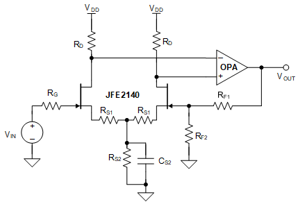
The JFE2140 can be configured to provide a low-noise, high-input impedance front-end stage for a typical op amp. Open-loop transistor gain stages shown previously suffer from wide gain variations that are dependent on the forward transcondutance of the JFE2140. When precision gain is required, the composite amplifier (JFET front-end + operational amplifier) achieves excellent results by allowing for a fixed gain determined by external resistors, and improving the noise and bandwidth of the operational amplifier. The JFE2140 gain stage provides a boost to the open-loop performance of the system, extending the bandwidth beyond what the operational amplifier alone can provide, and gives a high-input impedance, ultra-low noise input stage to interface with high source impedance microphones.
Figure 9-7 shows a generic schematic representation of a voltage-feedback composite amplifier. The component requirements and tradeoffs are listed in Table 9-1.
 Figure 9-6 Low Noise, High Input
Impedance Composite Amplifier
Figure 9-6 Low Noise, High Input
Impedance Composite AmplifierThe gain of Figure 9-7 can be calculated using the following equation:
| COMPONENT | DESCRIPTION |
|---|---|
| RS1 | Degeneration resistors. These resistors reduce the overall gain of the JFET stage, but improve the linearity performance. Also, when used in differential configurations (see OPA1637 reference design), the resistors reduce CMRR errors that occur as a result of input mismatch voltages. |
| RS2 | Bias-current setting resistor. This resistor, along with RS1, determine the bias current when using resistive biasing (see Figure 9-4). Be aware that both RS1 and RS2 resistance directly impact noise performance. |
| RG | Gate resistor. This resistor is used to help limit current flow into the gate in overvoltage cases. For improved dc precision, match RG to the equivalent parallel resistance of RS1 || RS2. Use the low resistance values to minimize the thermal noise impact on the circuit. |
| RD | Drain resistor. This resistor sets the JFET stage gain in common source biasing, along with gm and RS1 + RS2. Higher resistance increases gain, but lowers the nominal VDS voltage. |
| RF1 | Feedback resistor 1. Along with RF2, this resistor sets the gain of the composite amplifier. |
| RF2 | Feedback resistor 2. Along with RF1, this resistor sets the gain of the composite amplifier. |
| RS2 | Source resistor 2. Along with RS1, this resistor sets the dc bias current where the JFET is nominally operated. |
| CS | Source capacitor. This capacitor reduces the noise coupling from RS2. |