ZHCSM79 November 2020 INA280-Q1
PRODUCTION DATA
- 1 特性
- 2 应用
- 3 说明
- 4 Revision History
- 5 Pin Configuration and Functions
- 6 Specifications
- 7 Detailed Description
- 8 Application and Implementation
- 9 Power Supply Recommendations
- 10Layout
- 11Device and Documentation Support
- 12Mechanical, Packaging, and Orderable Information
7.3.1.1 Input-Signal Bandwidth
The INA280-Q1 –3-dB bandwidth is gain dependent with several gain options of 20 V/V, 50 V/V, 100 V/V, 200 V/V, and 500 V/V as shown in Figure 6-2. The unique multistage design enables the amplifier to achieve high bandwidth at all gains. This high bandwidth provides the throughput and fast response that is required for the rapid detection and processing of overcurrent events.
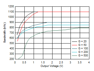
The bandwidth of the device also depends on the applied VSENSE voltage. Figure 7-2 shows the bandwidth performance profile of the device over frequency as output voltage increases for each gain variation. As shown in Figure 7-2, the device exhibits the highest bandwidth with higher VSENSE voltages, and the bandwidth is higher with lower device gain options. Individual requirements determine the acceptable limits of error for high-frequency, current-sensing applications. Testing and evaluation in the end application or circuit is required to determine the acceptance criteria and validate whether or not the performance levels meet the system specifications.

Figure 7-2 Bandwidth vs Output Voltage