ZHCSM79 November   2020 INA280-Q1

PRODUCTION DATA  

  1. 特性
  2. 应用
  3. 说明
  4. Revision History
  5. Pin Configuration and Functions
  6. Specifications
    1. 6.1 Absolute Maximum Ratings
    2. 6.2 ESD Ratings
    3. 6.3 Recommended Operating Conditions
    4. 6.4 Thermal Information
    5. 6.5 Electrical Characteristics
    6. 6.6 Typical Characteristics
  7. Detailed Description
    1. 7.1 Overview
    2. 7.2 Functional Block Diagram
    3. 7.3 Feature Description
      1. 7.3.1 Amplifier Input Common-Mode Range
        1. 7.3.1.1 Input-Signal Bandwidth
        2. 7.3.1.2 Low Input Bias Current
        3. 7.3.1.3 Multiple Fixed Gain Outputs
        4. 7.3.1.4 Wide Supply Range
    4. 7.4 Device Functional Modes
      1. 7.4.1 Unidirectional Operation
      2. 7.4.2 High Signal Throughput
  8. Application and Implementation
    1. 8.1 Application Information
      1. 8.1.1 RSENSE and Device Gain Selection
      2. 8.1.2 Input Filtering
    2. 8.2 Typical Application
      1. 8.2.1 Design Requirements
      2. 8.2.2 Detailed Design Procedure
        1. 8.2.2.1 Overload Recovery With Negative VSENSE
      3. 8.2.3 Application Curve
  9. Power Supply Recommendations
  10. 10Layout
    1. 10.1 Layout Guidelines
    2. 10.2 Layout Example
  11. 11Device and Documentation Support
    1. 11.1 Documentation Support
      1. 11.1.1 Related Documentation
    2. 11.2 接收文档更新通知
    3. 11.3 支持资源
    4. 11.4 Trademarks
    5. 11.5 静电放电警告
    6. 11.6 术语表
  12. 12Mechanical, Packaging, and Orderable Information

封装选项

机械数据 (封装 | 引脚)
散热焊盘机械数据 (封装 | 引脚)
订购信息

Typical Characteristics

All specifications at TA = 25 °C, VS = 5 V, VSENSE = VIN+ – VIN– = 0.5 V / Gain, and VCM = VIN– = 48 V, unless otherwise noted.
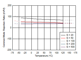

GUID-732E636E-AB44-4659-BBD7-5BDFF5A062A0-low.gif
Figure 6-1 Common-Mode Rejection Ratio vs Temperature
GUID-83CB5C14-B497-43EF-A4E1-8F6D47C4E244-low.gif
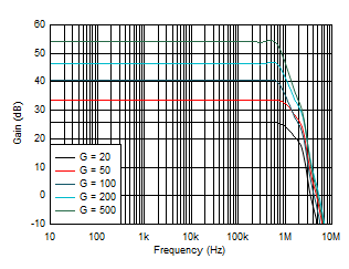
VSENSE = 4 V / Gain
Figure 6-3 Gain vs Frequency

GUID-EBF1063F-5008-40BB-9F20-20F122681385-low.gif
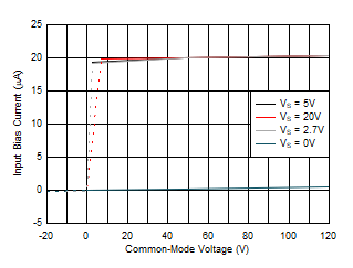
VSENSE = 0 V
Figure 6-5 Input Bias Current vs Common-Mode Voltage

GUID-48528101-06B8-4CB2-B01E-F0A7A0691DEB-low.gif
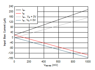
Figure 6-7 Input Bias Current vs VSENSE, A1 Devices
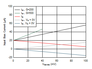
GUID-78D9677C-2552-443A-880C-67147AD98BB3-low.gif


Figure 6-9 Input Bias Current vs VSENSE, A4 and A5 Devices
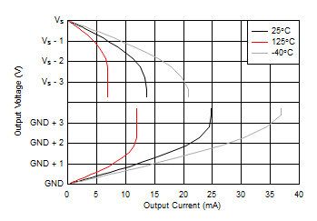
GUID-78527DC6-7EB1-4884-A2BD-4A0445F5B58F-low.gif
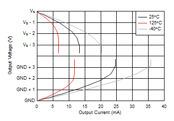
VS = 5 V
Figure 6-11 Output Voltage vs Output Current

GUID-A1C68206-E6E2-43F5-97FC-62B6BBCAF52E-low.gif


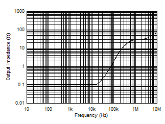
Figure 6-13 Output Impedance vs Frequency
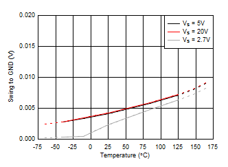
GUID-A7A94635-B310-4AD9-8492-A40CF8FEC4B2-low.gif
RL = 10 kΩ
Figure 6-15 Swing to GND vs Temperature

GUID-6957301E-4758-41A8-90A6-C5545E82A74A-low.gif
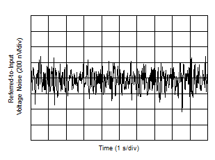
Figure 6-17 Input Referred Noise

GUID-89114D8A-87BD-4268-82FD-91E4CC6A2CCA-low.gif
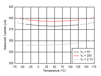
Figure 6-19 Quiescent Current vs Temperature
GUID-D8C6907D-B7BE-4540-A1AE-8C5ACA721707-low.gif
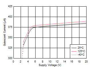
Figure 6-21 Quiescent Current vs Supply Voltage
GUID-670FFD46-4357-44AF-976A-EC26E2ED713A-low.gif
RL = 10 kΩ VSENSE = 5 mV
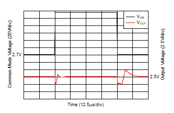
Figure 6-23 Common-Mode Voltage Fast Transient Pulse, A5 Devices

GUID-2874E55A-A346-4270-B11E-046DD345680A-low.gif
VSENSE = 0 mV
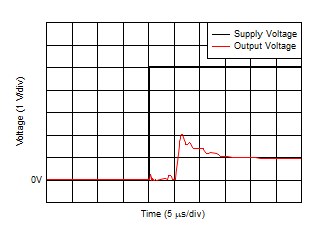
Figure 6-25 Start-Up Response

GUID-97D5B13C-307F-4152-BBB9-7A9A5D60E61F-low.gif
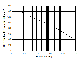
Figure 6-2 Common-Mode Rejection Ratio vs Frequency
GUID-C1528049-473A-496D-816B-CBA250497E65-low.gif


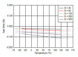
Figure 6-4 Gain Error vs Temperature

GUID-15960104-5DB9-4023-9D82-92F8DD9A5C03-low.gif


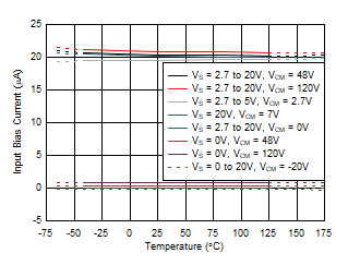
Figure 6-6 Input Bias Current vs Temperature
GUID-EF6B56BF-2E15-4A84-BF65-531646DAF701-low.gif
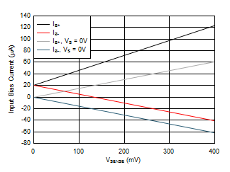
Figure 6-8 Input Bias Current vs VSENSE, A2 and A3 Devices
GUID-95BBE6DE-42CD-479A-959F-9DE1534035BE-low.gif
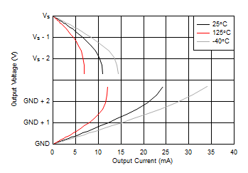
VS = 2.7 V
Figure 6-10 Output Voltage vs Output Current

GUID-23EEDE1D-E1D1-4ED6-A282-C036F7F4CBAA-low.gif
VS = 20 V
Figure 6-12 Output Voltage vs Output Current

GUID-563D842F-A7DE-4E11-B014-0487E967BF16-low.gif
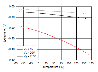
RL = 10 kΩ
Figure 6-14 Swing to Supply vs Temperature

GUID-CF196884-F84D-4102-9F03-1C43C12197CE-low.gif


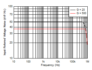
Figure 6-16 Input Referred Noise vs Frequency
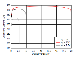
GUID-D58FEDFC-7BCF-42DA-B99C-1AD6988989F5-low.gif
Figure 6-18 Quiescent Current vs Output Voltage
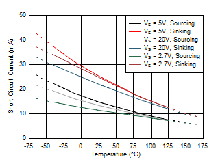
GUID-9205D467-FA04-464B-85C8-B5580FE0DE90-low.gif
Figure 6-20 Short-Circuit Current vs Temperature
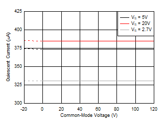
GUID-2633EED6-5871-41DA-9A83-2400F89DD812-low.gif
Figure 6-22 Quiescent Current vs Common-Mode Voltage
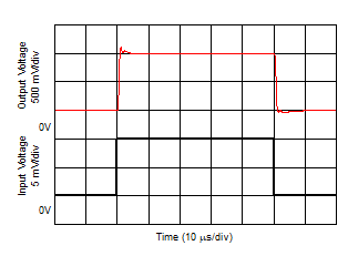
GUID-26D584DE-9A10-41BC-B98C-8E9530829B63-low.gif
Figure 6-24 Step Response, A3 Devices
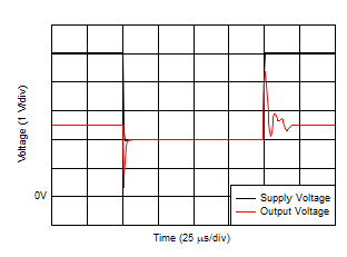
GUID-4C84526D-A338-4C67-9FBB-FB20C776D756-low.gif
VSENSE = 5 mV
Figure 6-26 Supply Transient Response, A5 Devices