ZHCSDQ8 April 2015 HD3SS2522
PRODUCTION DATA.
- 1 特性
- 2 应用
- 3 说明
- 4 简化电路原理图
- 5 修订历史记录
- 6 Pin Configuration and Functions
- 7 Specifications
- 8 Detailed Description
- 9 Application and Implementation
- 10Power Supply Recommendations
- 11Layout
- 12器件和文档支持
- 13机械、封装和可订购信息
7 Specifications
7.1 Absolute Maximum Ratings
over operating free-air temperature range (unless otherwise noted) (1)| MIN | MAX | UNIT | ||
|---|---|---|---|---|
| Power supply voltage range, VCC | –0.4 | 4 | V | |
| Voltage Range | Differential I/O (High bandwidth signal path, AxP/N, BxP/N, CxP/N) | –0.4 | 2.4 | |
| Control Pins and Single Ended I/Os including CC1 and CC2 | –0.4 | VCC + 0.4 | ||
(1) Stresses beyond those listed under Absolute Maximum Ratings may cause permanent damage to the device. These are stress ratings only, which do not imply functional operation of the device at these or any other conditions beyond those indicated under Recommended Operating Conditions. Exposure to absolute-maximum-rated conditions for extended periods may affect device reliability.
7.2 ESD Ratings
| VALUE | UNIT | |||
|---|---|---|---|---|
| V(ESD) | Electrostatic discharge | Human-body model (HBM), per ANSI/ESDA/JEDEC JS-001(1) | ±2000 | V |
| Charged-device model (CDM), per JEDEC specification JESD22-C101(2) | ±500 | |||
(1) JEDEC document JEP155 states that 500-V HBM allows safe manufacturing with a standard ESD control process.
(2) JEDEC document JEP157 states that 250-V CDM allows safe manufacturing with a standard ESD control process.
7.3 Recommended Operating Conditions
over operating free-air temperature range (unless otherwise noted)| MIN | NOM | MAX | UNIT | |||
|---|---|---|---|---|---|---|
| VCC | Supply voltage | 3 | 3.3 | 3.6 | V | |
| VIH | Input high voltage | Control/Status pins | 2 | VCC | V | |
| VIL | Input low voltage | Control/Status pins | –0.1 | 0.8 | V | |
| VI/O(Diff) | Differential voltage | Switch I/O diff voltage | 0 | 1.6 | VPP | |
| VI/O(CM) | Common voltage | Switch I/O common mode voltage | 0 | 2 | V | |
| VI/O | Input / output voltage | CC_OUT, CC_IN, and selected CC pin for configuration | 0 | VCC | V | |
| VIN | Input voltage | Selected CC pin for VCONN | 0 | 5.5 | V | |
| TA | Operating free-air temperature | HD3SS2522RHU | 0 | 70 | °C | |
7.4 Thermal Information
| THERMAL METRIC(1) | HD3SS2521A | UNIT | |
|---|---|---|---|
| RHU | |||
| 56 PINS | |||
| RθJA | Junction-to-ambient thermal resistance | 31.6 | °C/W |
| RθJC(top) | Junction-to-case (top) thermal resistance | 15.9 | |
| RθJB | Junction-to-board thermal resistance | 8.5 | |
| ψJT | Junction-to-top characterization parameter | 0.5 | |
| ψJB | Junction-to-board characterization parameter | 8.5 | |
| RθJC(bot) | Junction-to-case (bottom) thermal resistance | N/A | |
(1) For more information about traditional and new thermal metrics, see the IC Package Thermal Metrics application report, SPRA953.
7.5 Electrical Characteristics
over operating free-air temperature range (unless otherwise noted)| PARAMETER | TEST CONDITIONS | MIN | TYP | MAX | UNIT | |
|---|---|---|---|---|---|---|
| ICC | Supply current | VCC = 3.6 V, SS_OEn, CC_OEn = GND |
0.6 | 1 | mA | |
| I(STANDBY) | Standby current | VCC = 3.3 V, SS_OEN, CC_OEn = VCC | 15 | µA | ||
| VBUS_FAULT#, VCONN_FAULT#, IMODE1, IMODE2, RST, RSVD, GPIO1, GPIO2 | ||||||
| VIT+ | Positive-going input threshold voltage | 0.45 x VCC | 0.75 x VCC | V | ||
| VIT- | Negative-going input threshold voltage | 0.25 x VCC | 0.55 x VCC | V | ||
| Vhys | nput voltage hysteresis (VIT+ – VIT–) | VCC = 3 V | 0.3 | 1 | V | |
| RPULL | Pullup/pulldown resistor | Pullup: VIN = GND, Pulldown: VIN = VCC, VCC = 3 V |
20 | 35 | 50 | kΩ |
| CI | Input capacitance | VIN = GND or VCC | 5 | pF | ||
| ILGK | High-impedance leakage current | VIN = GND or VCC, VCC = 3 V, Pullup/Pulldown disabled |
±50 | nA | ||
| VCTRL1, VCTRL2, VBUS_EN | ||||||
| VOL | Low-level output voltage | IOL(max) = 6 mA (1) | GND + 0.3 | V | ||
| MODE_LED | ||||||
| VOH | High-level output voltage | IOH(max) = –6 mA (1) | VCC – 0.3 | V | ||
| VOL | Low-level output voltage | IOL(max) = 6 mA (1) | GND + 0.3 | V | ||
| AxP/N, BxP/N, CxP/N | ||||||
| ILGK | High-impedance leakage current | VCC = 3.6 V, VIN = 0 V, VOUT = 2 V (ILKG on open outputs Port B and C) |
130 | µA | ||
| VCC = 3.6 V, VIN = 0 V, VOUT = 2 V (ILKG on open outputs Port A) |
4 | µA | ||||
| CC1, CC2 | ||||||
| ILGK | High-impedance leakage current | VCC = 3.6 V, VIN = 0 V, VOUT = 0 V to 4 V |
1 | µA | ||
(1) The maximum total current, IOH(max) and IOL(max), for all outputs combined should not exceed ±48 mA to hold the maximum voltage drop specified.
7.6 Timing Requirements
| MIN | NOM | MAX | UNIT | |||
|---|---|---|---|---|---|---|
| AxP/N, BxP/N, CxP/N HIGH-BANDWIDTH SIGNAL PATH | ||||||
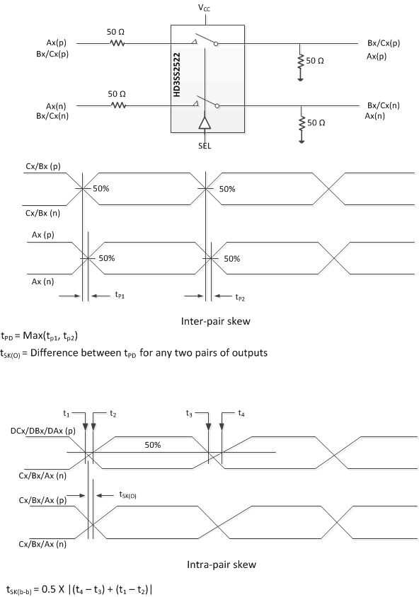
| tPD | Switch Propagation Delay | RSC and RL = 50 Ω | 85 | ps | ||
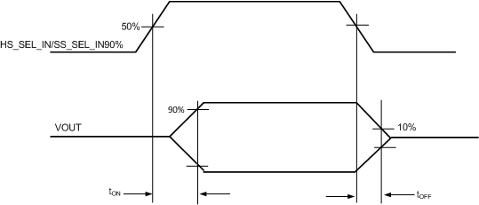
| tON | SS_SEL_IN -to-Switch tON | RSC and RL = 50 Ω | 70 | 250 | ns | |
| tOFF | SS_SEL_IN -to-Switch tOFF | 70 | 250 | ns | ||
 Figure 1. Select to Switch tON and tOFF

1. Measurements based on an ideal input with zero intra-pair skew on the input, i.e. the input at A to B/C or the input at B/C to A
2. Inter-pair skew is measured from lane to lane on the same channel, e.g. C0 to C1
3. Intra-pair skew is defined as the relative difference from the p and n signals of a single lane
Figure 2. Propagation Delay and Skew
7.7 Switching Characteristics
over operating free-air temperature range (unless otherwise noted)| PARAMETER | TEST CONDITIONS | MIN | TYP | MAX | UNIT | |
|---|---|---|---|---|---|---|
| AxP/N, BxP/N, CxP/N | ||||||
| tSK(O) | Inter-pair output skew (channel-channel) |
RSC and RL = 50 Ω | 20 | ps | ||
| tSK(b-b) | Inter-pair output skew (bit-bit) | 8 | ps | |||
| CON | Outputs ON capacitance | VIN = 0 V, outputs open, switch ON | 1.5 | pF | ||
| COFF | Outputs OFF capacitance | VIN = 0 V, outputs open, switch OFF | 1 | pF | ||
| RON | Output ON resistance | VCC = 3.3 V, VCM = 0.5 V – 1.5 V, IO = –8 mA |
5 | 8 | Ω | |
| ΔRON | On resistance match between channels | VCC = 3.3 V; –0.35 V ≤ VIN ≤ 1.2 V; IO = –8 mA |
2 | Ω | ||
| On resistance match between pairs of the same channel | 0.7 | |||||
| R(FLAT_ON) | On resistance flatness [RON(MAX) – RON(MIN)] |
VCC = 3.3 V; –0.35 V ≤ VIN ≤ 1.2 V | 1.15 | Ω | ||
| RL | Differential input return loss (VCM = 0 V) |
f = 2.5 GHz | –12 | dB | ||
| f = 4 GHz | –11 | |||||
| XTALK | Differential crosstalk (VCM = 0 V) | f = 2.5 GHz | –39 | dB | ||
| f = 4 GHz | –35 | |||||
| OIRR | Differential off-isolation (VCM = 0 V) | f = 2.5 GHz | –22 | dB | ||
| f = 4 GHz | –19 | |||||
| IL | Differential insertion loss (VCM = 0 V) |
f = 2.5 GHz | –1.1 | dB | ||
| f = 4 GHz | –1.5 | |||||
| BW | Bandwidth | At 3 dB | 6 | GHz | ||