ZHCSBO8A September 2013 – March 2014 DS125BR401A
PRODUCTION DATA.
- 1 特性
- 2 应用范围
- 3 说明
- 4 修订历史记录
- 5 Terminal Configuration and Functions
- 6 Specifications
- 7 Detailed Description
- 8 Applications and Implementation
- 9 Power Supply Recommendations
- 10Layout
- 11器件和文档支持
- 12机械封装和可订购信息
6 Specifications
6.1 Absolute Maximum Ratings(1)
| MIN | MAX | UNIT | ||
|---|---|---|---|---|
| Supply Voltage (VDD - 2.5V) | -0.5 | +2.75 | V | |
| Supply Voltage (VIN - 3.3V) | -0.5 | +4.0 | V | |
| LVCMOS Input/Output Voltage | -0.5 | +4.0 | V | |
| CML Input Voltage | -0.5V to (VDD+0.5) | |||
| CML Input Current | -30 | +30 | mA | |
(1) “Absolute Maximum Ratings” indicate limits beyond which damage to the device may occur, including inoperability and degradation of device reliability and/or performance. Functional operation of the device and/or non-degradation at the Absolute Maximum Ratings or other conditions beyond those indicated in the Recommended Operating Conditions is not implied. The Recommended Operating Conditions indicate conditions at which the device is functional and the device should not be operated beyond such conditions. Absolute Maximum Numbers are ensured for a junction temperature range of -40°C to +125°C. Models are validated to Maximum Operating Voltages only.
6.2 Handling Ratings
| MIN | MAX | UNIT | ||
|---|---|---|---|---|
| ESDHBM | HBM, STD - JESD22-A114F | 4 | kV | |
| ESDCDM | CDM, STD - JESD22-C101-D | 1 | kV | |
| Tstg | Storage Temperature Range | -40 | 125 | °C |
| Tsolder | Lead Temperature Range Soldering (4 sec.) (1) | 260 | °C |
(1) For soldering specifications: See application note SNOA549.
6.3 Recommended Operating Conditions
| MIN | TYP | MAX | UNIT | |
|---|---|---|---|---|
| Supply Voltage (2.5V mode) | 2.375 | 2.5 | 2.625 | V |
| Supply Voltage (3.3V mode) | 3.0 | 3.3 | 3.6 | V |
| Ambient Temperature | -40 | 25 | +85 | °C |
| SMBus (SDA, SCL) | 3.6 | V | ||
| Supply Noise up to 50 MHz(1) | 100 | mVp-p |
6.4 Thermal Information
| THERMAL METRIC(1) | DS125BR401A | UNIT | |
|---|---|---|---|
| WQFN | |||
| 54 TERMINALS | |||
| RθJA | Junction-to-ambient thermal resistance | 26.6 | °C/W |
| RθJCtop | Junction-to-case (top) thermal resistance | 10.8 | |
| RθJB | Junction-to-board thermal resistance | 4.4 | |
| ψJT | Junction-to-top characterization parameter | 0.2 | |
| ψJB | Junction-to-board characterization parameter | 4.3 | |
| RθJCbot | Junction-to-case (bottom) thermal resistance | 1.5 | |
(1) For more information about traditional and new thermal metrics, see the IC Package Thermal Metrics application report, SPRA953.
6.5 Electrical Characteristics
| PARAMETER | TEST CONDITIONS | MIN | TYP | MAX | UNIT | |
|---|---|---|---|---|---|---|
| POWER | ||||||
| IDD | Current Consumption | DEM0 = Float, ,DEM1 = Float EQ = 0, VOD = 0.8VP-P, RXDET = 1, PWDN = 0 |
200 | 280 | mA | |
| Power Down Current Consumption | PWDN = 1 | 14 | 27 | mA | ||
| VDD | Integrated LDO Regulator | VIN = 3.0 - 3.6 V | 2.375 | 2.5 | 2.625 | V |
| LVCMOS / LVTTL DC SPECIFICATIONS | ||||||
| Vih25 | High Level Input Voltage | 2.5 V Supply Mode | 1.7 | VDD | V | |
| Vih33 | High Level Input Voltage | 3.3 V Supply Mode | 1.7 | VIN | V | |
| Vil | Low Level Input Voltage | 0 | 0.7 | V | ||
| Voh | High Level Output Voltage (ALL_DONE Terminal) |
Ioh = −4mA | 2.0 | V | ||
| Vol | Low Level Output Voltage (ALL_DONE Terminal) |
Iol = 4mA | 0.4 | V | ||
| Iih | Input High Current (PWDN Terminal) | VIN = 3.6 V, LVCMOS = 3.6 V |
-15 | +15 | uA | |
| Iil | Input Low Current (PWDN Terminal) | VIN = 3.6 V, LVCMOS = 0 V |
-15 | +15 | uA | |
| 4-LEVEL INPUT DC SPECIFICATIONS | ||||||
| Iih | Input High Current with internal resistors (4–level input Terminal) |
VIN = 3.6 V, LVCMOS = 3.6 V |
+20 | +150 | uA | |
| Iil | Input Low Current with internal resistors (4–level input Terminal) |
VIN = 3.6 V, LVCMOS = 0 V |
-160 | -40 | uA | |
| Vth | Threshold 0 / R | VDD = 2.5V (2.5V supply mode) Internal LDO Disabled See Table 1 for details |
0.45 | V | ||
| Threshold R / Float | 1.2 | |||||
| Threshold Float / 1 | 2 | |||||
| Threshold 0 / R | VIN = 3.3V (3.3V supply mode) Internal LDO Enabled See Table 1 for details. |
0.6 | V | |||
| Threshold R / Float | 1.6 | |||||
| Threshold Float / 1 | 2.6 | |||||
| CML RECEIVER INPUTS (IN_n+, IN_n-) | ||||||
| RLRX-diff | RX Differential return loss | SDD11 10 MHz | -19 | dB | ||
| SDD11 2 GHz | -14 | |||||
| SDD11 6-11.1 GHz | -8 | |||||
| RLRX-cm | RX Common mode return loss | 0.05 - 5 GHz | -10 | dB | ||
| ZRX-dc | RX DC common mode impedance | Tested at VDD = 2.5 V | 40 | 50 | 60 | Ω |
| ZRX-diff-dc | RX DC differential mode impedance | Tested at VDD = 2.5 V | 80 | 100 | 120 | Ω |
| VRX-signal-det-diff-pp | Signal detect assert level for active data signal | SD_TH = F (float), 0101 pattern at 12 Gbps |
50 | mVp-p | ||
| VRX-idle-det-diff-pp | Signal detect de-assert level for electrical idle | SD_TH = F (float), 0101 pattern at 12 Gbps |
37 | mVp-p | ||
| HIGH SPEED OUTPUTS | ||||||
| TTX-RISE-FALL | Transmitter rise/fall time (3) | 20% to 80% of differential output voltage | 40 | ps | ||
| TRF-MISMATCH | Transmitter rise/fall mismatch | 20% to 80% of differential output voltage | 0.01 | UI | ||
| RLTX-DIFF | TX Differential return loss | SDD22 10 MHz - 2 GHz | -15 | dB | ||
| SDD22 5.5 GHz | -12 | |||||
| SDD22 11.1 GHz | -10 | dB | ||||
| RLTX-CM | TX Common mode return loss | 0.05 - 5 GHz | -10 | dB | ||
| ZTX-DIFF-DC | DC differential TX impedance | 100 | Ω | |||
| ITX-SHORT | Transmitter short circuit current limit | Total current, output shorted to VDD or GND | 20 | mA | ||
| VTX-CM-DC-ACTIVE-IDLE-DELTA | Absolute delta of DC common mode voltage during L0 and electrical idle | 100 | mV | |||
| VTX-CM-DC-LINE-DELTA | Absolute delta of DC common mode voltage between TX+ and TX- | 25 | mV | |||
| HIGH SPEED OUTPUTS (A-CHANNELS) | ||||||
| VTXA-diff1-pp | Output Voltage Differential Swing | Differential measurement with OUTA_n+ and OUTA_n-, AC-Coupled and terminated by 50Ω to GND, Inputs AC-Coupled, VID = 600 mVp-p VOD = 001'b (800mV) |
375 | 465 | 600 | mVp-p |
| VTXA-diff2-pp | Output Voltage Differential Swing | Differential measurement with OUTA_n+ and OUTA_n-, AC-Coupled and terminated by 50Ω to GND, Inputs AC-Coupled, VID = 1000 mVp-p VOD = 001'b (800mV) |
550 | 675 | 825 | mVp-p |
| VTXA-diff3-pp | Output Voltage Differential Swing | Differential measurement with OUTA_n+ and OUTA_n-, AC-Coupled and terminated by 50Ω to GND, Inputs AC-Coupled, VID = 600 mVp-p DEMA[1:0] = 10, VOD = 1300mV |
475 | 600 | 750 | Vp-p |
| VTXA-diff4-pp | Output Voltage Differential Swing | Differential measurement with OUTA_n+ and OUTA_n-, AC-Coupled and terminated by 50Ω to GND, Inputs AC-Coupled, VID = 1000 mVp-p VOD = 110'b (1300mV) |
775 | 915 | 1125 | Vp-p |
| TTXA-IDLE-DATA | Time to transition to valid differential signal after idle | VID = 1.0 Vp-p, 3 Gbps | 0.04 | ns | ||
| TTXA-DATA-IDLE | Time to transition to idle after differential signal | VID = 1.0 Vp-p, 3 Gbps | 0.70 | ns | ||
| TPDEQA | Differential propagation delay - Channel A | EQ = Level 1 to Level 4 | 80 | ps | ||
| HIGH SPEED OUTPUTS (B-CHANNELS) | ||||||
| VTXB-diff1-pp | Output Voltage Differential Swing | Differential measurement with OUTB_n+ and OUTB_n-, AC-Coupled and terminated by 50Ω to GND, Inputs AC-Coupled, VID = 1.0 Vp-p, MODE_B = 1 DEMB1 = 0, DEMB0 = 1(4) |
0.8 | 1.0 | 1.2 | Vp-p |
| VTXB-diff2-pp | Output Voltage Differential Swing | Differential measurement with OUTB_n+ and OUTB_n-, AC-Coupled and terminated by 50Ω to GND, Inputs AC-Coupled, VID = 1.0 Vp-p, MODE_B = 0 DEMB1 = 0, DEMB0 = R |
670 | 820 | 930 | mVp-p |
| VTXB-diff3-pp | Output Voltage Differential Swing | Differential measurement with OUTB_n+ and OUTB_n-, AC-Coupled and terminated by 50Ω to GND, Inputs AC-Coupled, VID = 1.0 Vp-p, MODE_B = 0 DEMB1 = R, DEMB0 = FLOAT |
950 | 1140 | 1250 | mVp-p |
| VTXB-de-ratio_3.5 | TX de-emphasis ratio | VOD = 1.0 Vp-p, DEM0 = 0, DEM1 = R, MODE_B = 0 OUTB_n only Gen 1 & 2 mode |
−3.5 | dB | ||
| VTXB-de-ratio_6 | TX de-emphasis ratio | VOD = 1.0 Vp-p, DEM0 = R, DEM1 = R, MODE_B = 0 OUTB_n only in Gen 1 & 2 mode |
−6 | dB | ||
| TTXB-IDLE-DATA | Time to transition to valid differential signal after idle | VID = 1.0 Vp-p, 3 Gbps | 3.5 | ns | ||
| TTXB-DATA-IDLE | Time to transition to idle after differential signal | VID = 1.0 Vp-p, 3 Gbps | 5.0 | ns | ||
| TPDEQB | Differential propagation delay - Channel B | EQ = 00(2) | 135 | ps | ||
| EQUALIZATION (A-CHANNELS) | ||||||
| DJE1A | Residual deterministic jitter at 6 Gbps | 5” Differential Stripline, 5mil trace width, FR4, VID = 0.8 Vp-p, PRBS15, EQ = 01'h, VOD = 1.3V, DEM = 0 dB |
0.06 | UI | ||
| DJE3A | Residual deterministic jitter at 12 Gbps | 5” Differential Stripline, 5mil trace width, FR4, VID = 0.8 Vp-p, PRBS15, EQ = 01'h, VOD = 1.3V, DEM = 0 dB |
0.12 | UI | ||
| EQUALIZATION (B-CHANNELS) | ||||||
| DJE1B | Residual deterministic jitter at 12 Gbps | 30” Differential Stripline, 5mil trace width, FR4, VID = 0.6 Vp-p, PRBS15, EQ = 07'h, DEM = 0 dB |
0.18 | UI | ||
| DJE2B | Residual deterministic jitter at 12 Gbps | 5 meters 30 awg cable, VID = 0.6 Vp-p, PRBS15, EQ = 07'h, DEM = 0 dB |
0.25 | UI | ||
| DE-EMPHASIS (B-CHANNELS, GEN 1&2 MODE ONLY) | ||||||
| DJD1 | Residual deterministic jitter at 12 Gbps |
Input Channel: 20" Differential Stripline, 5mil trace width, FR4, Output Channel: 10” Differential Stripline, 5mil trace width, FR4, VID = 0.6 Vp-p, PRBS15, EQ = 03'h, VOD = 1.0 Vp-p, DEMB = −3.5 dB |
0.1 | UI | ||
(1) Allowed supply noise (mVp-p sine wave) under typical conditions.
(2) Propagation Delay measurements will change slightly based on the level of EQ selected. EQ = 00 will result in the shortest propagation delays.
(3) Rise / Fall time measurements will on A-Channels will vary based on EQ setting, Input Amplitude, and input edge rate.
(4) In SAS-3 and PCIe GEN3 mode, the output VOD level is not fixed. It will be adjusted automatically based on the VID input amplitude level. The output VOD level set by DEMA/B[1:0] in this mode BOUTn is dependent on the VID level and the frequency content. The DS125BR401A repeater is designed to be transparent in this mode, so the TX-FIR (de-emphasis) is passed to the RX to support the handshake negotiation link training.
6.6 Electrical Characteristics — Serial Management Bus Interface
Over recommended operating supply and temperature ranges unless other specified.| PARAMETER | TEST CONDITIONS | MIN | TYP | MAX | UNIT | |
|---|---|---|---|---|---|---|
| SERIAL BUS INTERFACE DC SPECIFICATIONS | ||||||
| VIL | Data, Clock Input Low Voltage | 0.8 | V | |||
| VIH | Data, Clock Input High Voltage | 2.1 | 3.6 | V | ||
| VOL | Output Low Voltage | SDA or SCL, IOL = 1.25 mA | 0 | 0.36 | V | |
| VDD | Nominal Bus Voltage | 2.375 | 3.6 | V | ||
| IIH-Terminal | Input Leakage Per Device Terminal | +20 | +150 | µA | ||
| IIL-Terminal | Input Leakage Per Device Terminal | -160 | -40 | µA | ||
| CI | Capacitance for SDA and SCL | See(1)(2) | < 5 | pF | ||
| RTERM | External Termination Resistance pull to VDD = 2.5V ± 5% OR 3.3V ± 10% | Pullup VDD = 3.3V(1)(2)(3) | 2000 | Ω | ||
| Pullup VDD = 2.5V(1)(2)(3) | 1000 | Ω | ||||
(1) Recommended value.
(2) Recommended maximum capacitance load per bus segment is 400pF.
(3) Maximum termination voltage should be identical to the device supply voltage.
6.7 Timing Requirements Serial Bus Interface
| PARAMETER | TEST CONDITIONS | MIN | TYP | MAX | UNIT | |
|---|---|---|---|---|---|---|
| SERIAL BUS INTERFACE TIMING SPECIFICATIONS | ||||||
| FSMB | Bus Operating Frequency | ENSMB = VDD (Slave Mode) | 400 | kHz | ||
| ENSMB = FLOAT (Master Mode) | 280 | 400 | 520 | kHz | ||
| tFALL | SDA Fall Time | Read operation RPU = 4.7K, Cb < 50pF |
60 | ns | ||
| tRISE | SDA Rise Time | Read operation RPU = 4.7K, Cb < 50pF |
140 | ns | ||
| tF | Clock/Data Fall Time | See(1) | 300 | ns | ||
| tR | Clock/Data Rise Time | See(1) | 1000 | ns | ||
(1) Compliant to SMBus 2.0 physical layer specification. See System Management Bus (SMBus) Specification Version 2.0, section 3.1.1 SMBus common AC specifications for details.
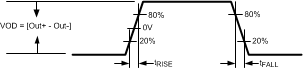 Figure 1. Output and Rise And Fall Transition Time
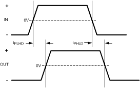 Figure 2. Propagation Delay Timing Diagram
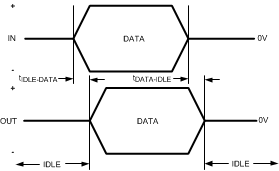 Figure 3. Transmit Idle-Data and Data-Idle Response Time
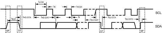 Figure 4. SMBus Timing Parameters
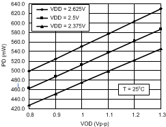
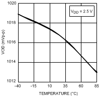
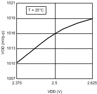
6.8 Typical Characteristics