ZHCSBO8A September 2013 – March 2014 DS125BR401A
PRODUCTION DATA.
- 1 特性
- 2 应用范围
- 3 说明
- 4 修订历史记录
- 5 Terminal Configuration and Functions
- 6 Specifications
- 7 Detailed Description
- 8 Applications and Implementation
- 9 Power Supply Recommendations
- 10Layout
- 11器件和文档支持
- 12机械封装和可订购信息
10 Layout
10.1 Layout Guidelines
The CML inputs and outputs have been optimized to work with interconnects using a controlled differential impedance of 100Ω. It is preferable to route differential lines exclusively on one layer of the board, particularly for the input traces. The use of vias should be avoided if possible. If vias must be used, they should be used sparingly and must be placed symmetrically for each side of a given differential pair. Whenever differential vias are used the layout must also provide for a low inductance path for the return currents as well. Route the differential signals away from other signals and noise sources on the printed circuit board. See AN-1187 “Leadless Leadframe Package (LLP) Application Report” (literature number SNOA401) for additional information on QFN (WQFN) packages.
10.2 Layout Example
To minimize the effects of crosstalk, a 5:1 ratio or greater should be maintained between inter-pair and intra-pair spacing.
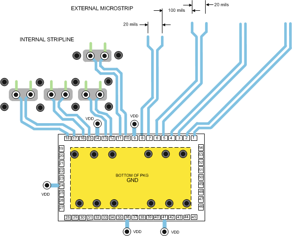 Figure 22. Typical Routing Options
The graphic shown above depicts different transmission line topologies which can be used in various combinations to achieve the optimal system performance. Impedance discontinuities at the differential via can be minimized or eliminated by increasing the swell around each hole and providing for a low inductance return current path. When the via structure is associated with thick backplane PCB, further optimization such as back drilling is often used to reduce the detrimental high frequency effects of stubs on the signal path.