ZHCSBO8A September 2013 – March 2014 DS125BR401A
PRODUCTION DATA.
- 1 特性
- 2 应用范围
- 3 说明
- 4 修订历史记录
- 5 Terminal Configuration and Functions
- 6 Specifications
- 7 Detailed Description
- 8 Applications and Implementation
- 9 Power Supply Recommendations
- 10Layout
- 11器件和文档支持
- 12机械封装和可订购信息
5 Terminal Configuration and Functions
54-Lead WQFN
Top View
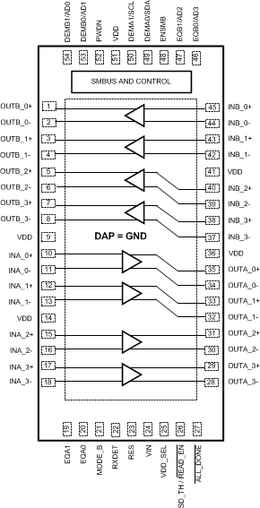
A. Above 54-lead WQFN graphic is a TOP VIEW, looking down through the package.
Terminal Functions(1)
| TERMINAL NAME | TERMINAL NUMBER | I/O, TYPE | TERMINAL DESCRIPTION |
|---|---|---|---|
| DIFFERENTIAL HIGH SPEED I/O | |||
| INB_0+, INB_0- , INB_1+, INB_1-, INB_2+, INB_2-, INB_3+, INB_3- |
45, 44, 43, 42 40, 39, 38, 37 |
I | Inverting and non-inverting CML differential inputs to the equalizer. On-chip 50Ω termination resistor connects INB_n+ to VDD and INB_n- to VDD when enabled. AC coupling required on high-speed I/O |
| OUTB_0+, OUTB_0-, OUTB_1+, OUTB_1-, OUTB_2+, OUTB_2-, OUTB_3+, OUTB_3- |
1, 2, 3, 4 5, 6, 7, 8 |
O | Inverting and non-inverting 50Ω driver outputs with de-emphasis. Compatible with AC coupled CML inputs. AC coupling required on high-speed I/O |
| INA_0+, INA_0- , INA_1+, INA_1-, INA_2+, INA_2-, INA_3+, INA_3- |
10, 11, 12, 13 15, 16, 17, 18 |
I | Inverting and non-inverting CML differential inputs to the equalizer. On-chip 50Ω termination resistor connects INA_n+ to VDD and INA_n- to VDD when enabled. AC coupling required on high-speed I/O |
| OUTA_0+, OUTA_0-, OUTA_1+, OUTA_1-, OUTA_2+, OUTA_2-, OUTA_3+, OUTA_3- |
35, 34, 33, 32 31, 30, 29, 28 |
O | Inverting and non-inverting 50Ω driver outputs. Compatible with AC coupled CML inputs. AC coupling required on high-speed I/O |
| CONTROL TERMINALS — SHARED (LVCMOS) | |||
| ENSMB | 48 | I, LVCMOS | System Management Bus (SMBus) enable Terminal Tie 1kΩ to VDD = Register Access SMBus Slave mode FLOAT = Read External EEPROM (Master SMBUS Mode) Tie 1kΩ to GND = Terminal Mode |
| ENSMB = 1 (SMBus MODE) | |||
| SCL | 50 | I, LVCMOS, O, OPEN Drain |
ENSMB Master or Slave mode SMBus clock input Terminal is enabled (slave mode). Clock output when loading EEPROM configuration (master mode). |
| SDA | 49 | I, LVCMOS, O, OPEN Drain |
ENSMB Master or Slave mode The SMBus bidirectional SDA Terminal is enabled. Data input or open drain (pull-down only) output. |
| AD0-AD3 | 54, 53, 47, 46 | I, LVCMOS | ENSMB Master or Slave mode SMBus Slave Address Inputs. In SMBus mode, these Terminals are the user set SMBus slave address inputs. |
| READ_EN | 26 | I, LVCMOS | When using an External EEPROM, a logic low on this terminal starts the load from the external EEPROM |
| ENSMB = 0 (TERMINAL MODE) | |||
| EQA0, EQA1 EQB0, EQB1 |
20, 19 46, 47 |
I, 4-LEVEL, LVCMOS |
EQA[1:0] and EQB[1:0] control the level of equalization of the A/B directions. The Terminals are defined as EQx[1:0] only when ENSMB is de-asserted (low). Each of the 4 A/B channels have the same level unless controlled by the SMBus control registers. When ENSMB goes high the SMBus registers provide independent control of each lane. The EQB[1:0] Terminals are converted to SMBus AD2, AD3 inputs. See Table 5. |
| DEMB0, DEMB1 | 53, 54 | I, 4-LEVEL, LVCMOS |
DEMB[1:0] controls the level of de-emphasis of CHB outputs. The Terminals are defined as DEMB[1:0] only when ENSMB is de-asserted (low). Each of the 4 B channels have the same level unless controlled by the SMBus control registers. When ENSMB goes high the SMBus registers provide independent control of each lane. The DEMB[1:0] Terminals are converted to AD0, AD1 inputs. See Table 7. |
| MODE_B | 21 | I, 4-LEVEL, LVCMOS |
MODE_B control Terminal selects operating modes for the INB-OUTB Channels. Tie 1kΩ to GND = GEN 1,2 and SAS 1,2 Float = Auto Mode Select (for PCIe) Tie 20kΩ to GND = SAS-3 and GEN-3 without De-emphasis Tie 1kΩ to VDD = SAS-3 and GEN-3 with De-emphasis See Table 4. |
| DEMA0, DEMA1 | 49, 50 | I, 4-LEVEL, LVCMOS |
DEMA[1:0] controls the CHA output amplitude. The Terminals are defined as DEMA[1:0] only when ENSMB is de-asserted (low). Each of the 4 A channels have the same level unless controlled by the SMBus control registers. When ENSMB goes high the SMBus registers provide independent control of each lane and the DEMA[1:0] Terminals are converted to SCL and SDA. See Table 7. |
| SD_TH | 26 | I, 4-LEVEL, LVCMOS |
Controls the internal Signal Detect Threshold on the INB-OUTB Channels. For CHB, the signal detect is used to bring the output into and out of IDLE. This allows the OOB signaling to pass with minimal distortion. See Table 3. |
| CONTROL TERMINALS — BOTH TERMINAL AND SMBus MODES (LVCMOS) | |||
| RXDET | 22 | I, 4-LEVEL, LVCMOS |
The RXDET Terminal controls the receiver detect function. Depending on the input level, a 50Ω or >50KΩ termination to the power rail is enabled. In SAS/SATA system RXDET should be set to a Logic "1" state to keep the termination always enabled. See Table 2. |
| RES | 23 | I, 4-LEVEL, LVCMOS |
Reserved: This input must be left Floating. |
| VDD_SEL | 25 | I, FLOAT | Controls the internal regulator Float = 2.5V mode Tie GND = 3.3V mode |
| PWDN | 52 | I, LVCMOS | Tie High = Low power - power down Tie GND = Normal Operation See Table 2. |
| ALL_DONE | 27 | O, LVCMOS | Valid Register Load Status Output HIGH = External EEPROM load failed or incomplete LOW = External EEPROM load passed |
| POWER | |||
| VIN | 24 | Power | In 3.3V mode, feed 3.3V to VIN In 2.5V mode, leave floating. |
| VDD | 9, 14,36, 41, 51 | Power | Power supply Terminals CML/analog 2.5V mode, connect to 2.5V 3.3V mode, connect 0.1 µF cap to each VDD Terminal and GND |
| GND | DAP | Power | Ground pad (DAP - die attach pad). |
(1) LVCMOS inputs without the “Float” conditions must be driven to a logic low or high at all times or operation is not ensured.
Input edge rate for LVCMOS/FLOAT inputs must be faster than 50 ns from 10–90%.
For 3.3V mode operation, VIN Terminal input = 3.3V and the logic "1" reference for the 4-level input is 3.3V.
For 2.5V mode operation, VDD Terminal output= 2.5V and the logic "1" reference for the 4-level input is 2.5V.
Input edge rate for LVCMOS/FLOAT inputs must be faster than 50 ns from 10–90%.
For 3.3V mode operation, VIN Terminal input = 3.3V and the logic "1" reference for the 4-level input is 3.3V.
For 2.5V mode operation, VDD Terminal output= 2.5V and the logic "1" reference for the 4-level input is 2.5V.