ZHCSC12D November   2013  – October 2019 DRV8850

PRODUCTION DATA.  

  1. 特性
  2. 应用范围
  3. 说明
    1.     Device Images
      1.      简化原理图
  4. 修订历史记录
  5. Pin Configuration and Functions
    1.     Pin Functions
  6. Specifications
    1. 6.1 Absolute Maximum Ratings
    2. 6.2 ESD Ratings
    3. 6.3 Recommended Operating Conditions
    4. 6.4 Thermal Information
    5. 6.5 Electrical Characteristics
    6. 6.6 Timing Requirements
    7. 6.7 Typical Characteristics
  7. Detailed Description
    1. 7.1 Overview
    2. 7.2 Functional Block Diagram
    3. 7.3 Feature Description
      1. 7.3.1 Power Supervisor
      2. 7.3.2 Bridge Control
      3. 7.3.3 Current Sensing – VPROPI
      4. 7.3.4 Slew-Rate Control
      5. 7.3.5 Dead Time
      6. 7.3.6 Propagation Delay
      7. 7.3.7 Power Supplies and Input Pins
      8. 7.3.8 LDO Voltage Regulator
      9. 7.3.9 Protection Circuits
        1. 7.3.9.1 Overcurrent Protection (OCP)
        2. 7.3.9.2 Thermal Shutdown (TSD)
        3. 7.3.9.3 Undervoltage Lockout (UVLO)
        4. 7.3.9.4 Overvoltage Lockout (OVLO)
    4. 7.4 Device Functional Modes
  8. Application and Implementation
    1. 8.1 Application Information
    2. 8.2 Typical Application
      1. 8.2.1 Design Requirements
      2. 8.2.2 Detailed Design Procedure
        1. 8.2.2.1 Motor Voltage
        2. 8.2.2.2 Drive Current
      3. 8.2.3 Application Curves
  9. Power Supply Recommendations
    1. 9.1 Bulk Capacitance
  10. 10Layout
    1. 10.1 Layout Guidelines
    2. 10.2 Layout Example
    3. 10.3 Thermal Considerations
      1. 10.3.1 Power Dissipation
  11. 11器件和文档支持
    1. 11.1 文档支持
      1. 11.1.1 相关文档
    2. 11.2 接收文档更新通知
    3. 11.3 社区资源
    4. 11.4 商标
    5. 11.5 静电放电警告
    6. 11.6 Glossary
  12. 12机械、封装和可订购信息

封装选项

机械数据 (封装 | 引脚)
散热焊盘机械数据 (封装 | 引脚)
订购信息

Typical Characteristics

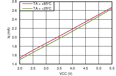
DRV8850 C001_SLVSCC0.png
Figure 1. Quiescent Current With Motor Driver ON and LDO ON
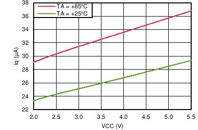
DRV8850 C003_SLVSCC0.png
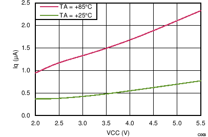
Figure 3. Quiescent Current With Motor Driver OFF and LDO ON
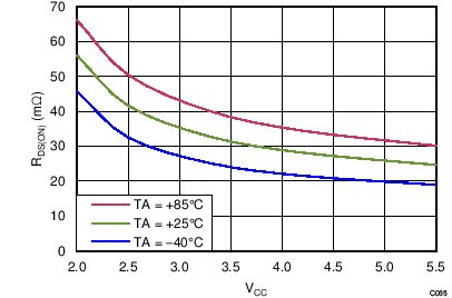
DRV8850 C005_SLVSCC0.png
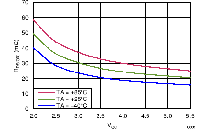
Figure 5. RDS(ON), HS – OUT1
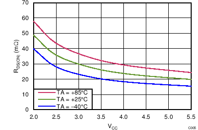
DRV8850 C007_SLVSCC0.png
Figure 7. RDS(ON), LS – OUT1
DRV8850 C009_SLVSCC0.png
Figure 9. LDO Output, VCC = 3.5 V,
LDOOUT = 3.3 V
DRV8850 C011_SLVSCC0.png
Figure 11. LDO Output, VCC = 5.5 V,
LDOOUT = 3.3 V
DRV8850 C013_SLVSCC0.png
Figure 13. VPROPI Output, VCC = 4.2 V, OUT2 Overtemperature, 1 kΩ
DRV8850 C002_SLVSCC0.png
Figure 2. Quiescent Current With Motor Driver ON and LDO OFF
DRV8850 C004_SLVSCC0.png
Figure 4. Quiescent Current With Motor Driver OFF and LDO OFF, Sleep Current
DRV8850 C006_SLVSCC0.png
Figure 6. RDS(ON), HS – OUT2
DRV8850 C008_SLVSCC0.png
Figure 8. RDS(ON), LS – OUT2
DRV8850 C010_SLVSCC0.png
Figure 10. LDO Output, VCC = 4.2 V,
LDOOUT = 3.3 V
DRV8850 C012_SLVSCC0.png
Figure 12. VPROPI Output, VCC = 4.2 V, OUT1 Overtemperature, 1 kΩ