ZHCSNT9K July 2008 – March 2021 DRV8800 , DRV8801
PRODUCTION DATA
- 1 特性
- 2 应用
- 3 说明
- 4 Revision History
- 5 Pin Configuration and Functions
- 6 Specifications
- 7 Parameter Measurement Information
- 8 Detailed Description
- 9 Application and Implementation
- 10Power Supply Recommendations
- 11Layout
- 12Device and Documentation Support
- 13Mechanical, Packaging, and Orderable Information
封装选项
机械数据 (封装 | 引脚)
散热焊盘机械数据 (封装 | 引脚)
订购信息
5 Pin Configuration and Functions
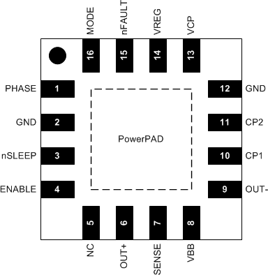
 Figure 5-1 DRV8800 RTY Package16-Pin WQFNTop View
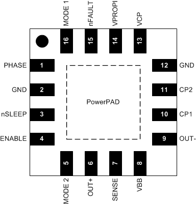
 Figure 5-2 DRV8801 RTY Package16-Pin WQFNTop View
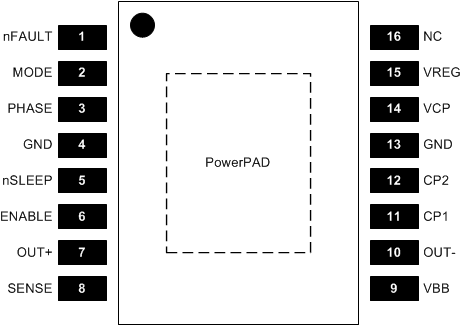
 Figure 5-3 DRV8800 PWP Package16-Pin HTSSOPTop View
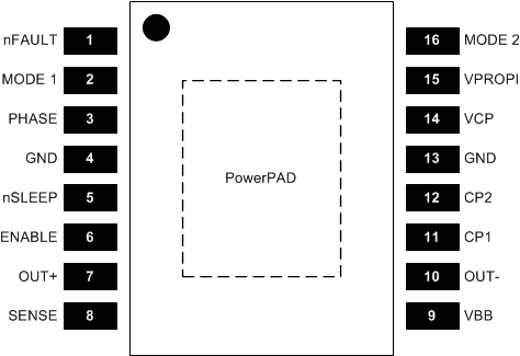
 Figure 5-4 DRV8801 PWP Package16-Pin HTSSOPTop View
Table 5-1 Pin Functions
| PIN | I/O | DESCRIPTION | ||||
|---|---|---|---|---|---|---|
| NAME | DRV8800 | DRV8801 | ||||
| WQFN | HTSSOP | WQFN | HTSSOP | |||
| CP1 | 10 | 11 | 10 | 11 | P | Charge pump switching node. Connect a 0.1-μF X7R ceramic capacitor rated for VBB between CP1 and CP2. |
| CP2 | 11 | 12 | 11 | 12 | P | Charge pump switching node. Connect a 0.1-μF X7R ceramic capacitor rated for VBB between CP1 and CP2. |
| ENABLE | 4 | 6 | 4 | 6 | I | Enable logic input. Set high to enable the H-bridge. |
| GND | 2,12 | 4, 13 | 2, 12 | 4, 13 | P | Device ground |
| MODE | 16 | 2 | — | — | I | Mode logic input |
| MODE 1 | — | — | 16 | 2 | I | Mode logic input |
| MODE 2 | — | — | 5 | 16 | I | Mode 2 logic input |
| NC | 5 | 16 | — | — | NC | No connect |
| nFAULT | 15 | 1 | 15 | 1 | OD | Fault indication. Pulled logic low with fault condition; open-drain output requires an external pullup resistor. |
| nSLEEP | 3 | 5 | 3 | 5 | I | Sleep mode input. Logic high to enable device; logic low to enter low-power sleep mode; internal pulldown resistor. |
| OUT+ | 6 | 7 | 6 | 7 | O | DMOS H-bridge output. Connect to motor terminal. |
| OUT- | 9 | 10 | 9 | 10 | O | DMOS H-bridge output. Connect to motor terminal. |
| PHASE | 1 | 3 | 1 | 3 | I | WQFN Package: Phase logic input for direction control. HTSSOP Package: Phase logic input. Controls the direction of the H-bridge. |
| SENSE | 7 | 8 | 7 | 8 | O (DRV8800) IO (DRV8801) |
Sense Power Return |
| VBB | 8 | 9 | 8 | 9 | P | Driver supply voltage. Bypass to GND with 0.1-μF ceramic capacitors plus a bulk capacitor rated for VBB. |
| VCP | 13 | 14 | 13 | 14 | P | Charge pump reservoir capacitor pin. Connect a X7R, 0.1-μF, 16-V ceramic capacitor to VBB. |
| VREG | 14 | 15 | — | — | P | Regulated voltage. |
| VPROPI | — | — | 14 | 15 | O | Voltage output proportional to winding current. |
| PowerPAD | — | — | — | — | — | Exposed pad for thermal dissipation. Connect to ground. |