ZHCSR67 July   2020 DRV8353M

PRODUCTION DATA  

  1. 特性
  2. 应用
  3. 说明
  4. Revision History
  5. Device Comparison Table
  6. Pin Configuration and Functions
    1.     Pin Functions—40-Pin DRV8353M Devices
  7. Absolute Maximum Ratings
  8. ESD Ratings
  9. Recommended Operating Conditions
  10. 10Thermal Information
  11. 11Electrical Characteristics
  12. 12SPI Timing Requirements
  13. 13Detailed Description
    1. 13.1 Overview
    2. 13.2 Functional Block Diagram
    3. 13.3 Feature Description
      1. 13.3.1 Three Phase Smart Gate Drivers
        1. 13.3.1.1 PWM Control Modes
          1. 13.3.1.1.1 6x PWM Mode (PWM_MODE = 00b or MODE Pin Tied to AGND)
          2. 13.3.1.1.2 3x PWM Mode (PWM_MODE = 01b or MODE Pin = 47 kΩ to AGND)
          3. 13.3.1.1.3 1x PWM Mode (PWM_MODE = 10b or MODE Pin = Hi-Z)
          4. 13.3.1.1.4 Independent PWM Mode (PWM_MODE = 11b or MODE Pin Tied to DVDD)
        2. 13.3.1.2 Device Interface Modes
          1. 13.3.1.2.1 Serial Peripheral Interface (SPI)
          2. 13.3.1.2.2 Hardware Interface
        3. 13.3.1.3 Gate Driver Voltage Supplies and Input Supply Configurations
        4. 13.3.1.4 Smart Gate Drive Architecture
          1. 13.3.1.4.1 IDRIVE: MOSFET Slew-Rate Control
          2. 13.3.1.4.2 TDRIVE: MOSFET Gate Drive Control
          3. 13.3.1.4.3 Propagation Delay
          4. 13.3.1.4.4 MOSFET VDS Monitors
          5. 13.3.1.4.5 VDRAIN Sense and Reference Pin
      2. 13.3.2 DVDD Linear Voltage Regulator
      3. 13.3.3 Pin Diagrams
      4. 13.3.4 Low-Side Current-Shunt Amplifiers
        1. 13.3.4.1 Bidirectional Current Sense Operation
        2. 13.3.4.2 Unidirectional Current Sense Operation (SPI only)
        3. 13.3.4.3 Amplifier Calibration Modes
        4. 13.3.4.4 MOSFET VDS Sense Mode (SPI Only)
      5. 13.3.5 Gate Driver Protective Circuits
        1. 13.3.5.1 VM Supply and VDRAIN Undervoltage Lockout (UVLO)
        2. 13.3.5.2 VCP Charge-Pump and VGLS Regulator Undervoltage Lockout (GDUV)
        3. 13.3.5.3 MOSFET VDS Overcurrent Protection (VDS_OCP)
          1. 13.3.5.3.1 VDS Latched Shutdown (OCP_MODE = 00b)
          2. 13.3.5.3.2 VDS Automatic Retry (OCP_MODE = 01b)
          3. 13.3.5.3.3 VDS Report Only (OCP_MODE = 10b)
          4. 13.3.5.3.4 VDS Disabled (OCP_MODE = 11b)
        4. 13.3.5.4 VSENSE Overcurrent Protection (SEN_OCP)
          1. 13.3.5.4.1 VSENSE Latched Shutdown (OCP_MODE = 00b)
          2. 13.3.5.4.2 VSENSE Automatic Retry (OCP_MODE = 01b)
          3. 13.3.5.4.3 VSENSE Report Only (OCP_MODE = 10b)
          4. 13.3.5.4.4 VSENSE Disabled (OCP_MODE = 11b or DIS_SEN = 1b)
        5. 13.3.5.5 Gate Driver Fault (GDF)
        6. 13.3.5.6 Overcurrent Soft Shutdown (OCP Soft)
        7. 13.3.5.7 Thermal Warning (OTW)
        8. 13.3.5.8 Thermal Shutdown (OTSD)
        9. 13.3.5.9 Fault Response Table
    4. 13.4 Device Functional Modes
      1. 13.4.1 Gate Driver Functional Modes
        1. 13.4.1.1 Sleep Mode
        2. 13.4.1.2 Operating Mode
        3. 13.4.1.3 Fault Reset (CLR_FLT or ENABLE Reset Pulse)
    5. 13.5 Programming
      1. 13.5.1 SPI Communication
        1. 13.5.1.1 SPI
          1. 13.5.1.1.1 SPI Format
    6. 13.6 Register Maps
      1. 13.6.1 Status Registers
        1. 13.6.1.1 Fault Status Register 1 (address = 0x00h)
        2. 13.6.1.2 Fault Status Register 2 (address = 0x01h)
      2. 13.6.2 Control Registers
        1. 13.6.2.1 Driver Control Register (address = 0x02h)
        2. 13.6.2.2 Gate Drive HS Register (address = 0x03h)
        3. 13.6.2.3 Gate Drive LS Register (address = 0x04h)
        4. 13.6.2.4 OCP Control Register (address = 0x05h)
        5. 13.6.2.5 CSA Control Register (address = 0x06h)
        6. 13.6.2.6 Driver Configuration Register (address = 0x07h)
  14. 14Application and Implementation
    1. 14.1 Application Information
    2. 14.2 Typical Application
      1. 14.2.1 Primary Application
        1. 14.2.1.1 Design Requirements
        2. 14.2.1.2 Detailed Design Procedure
          1. 14.2.1.2.1 External MOSFET Support
            1. 14.2.1.2.1.1 MOSFET Example
          2. 14.2.1.2.2 IDRIVE Configuration
            1. 14.2.1.2.2.1 IDRIVE Example
          3. 14.2.1.2.3 VDS Overcurrent Monitor Configuration
            1. 14.2.1.2.3.1 VDS Overcurrent Example
          4. 14.2.1.2.4 Sense-Amplifier Bidirectional Configuration
            1. 14.2.1.2.4.1 Sense-Amplifier Example
          5. 14.2.1.2.5 Single Supply Power Dissipation
          6. 14.2.1.2.6 Single Supply Power Dissipation Example
        3. 14.2.1.3 Application Curves
  15. 15Power Supply Recommendations
    1. 15.1 Bulk Capacitance Sizing
  16. 16Layout
    1. 16.1 Layout Guidelines
    2. 16.2 Layout Example
  17. 17Device and Documentation Support
    1. 17.1 Device Support
      1. 17.1.1 Device Nomenclature
    2. 17.2 Documentation Support
      1. 17.2.1 Related Documentation
    3. 17.3 Receiving Notification of Documentation Updates
    4. 17.4 Support Resources
    5. 17.5 Trademarks
    6. 17.6 Electrostatic Discharge Caution
    7. 17.7 Glossary
  18. 18Mechanical, Packaging, and Orderable Information

封装选项

机械数据 (封装 | 引脚)
散热焊盘机械数据 (封装 | 引脚)
订购信息

DVDD Linear Voltage Regulator

A 5-V, 10-mA linear regulator is integrated into the DRV8353M family of devices and is available for use by external circuitry. This regulator can provide the supply voltage for low-current supporting circuitry. The output of the DVDD regulator should be bypassed near the DVDD pin with a X5R or X7R, 1-µF, 6.3-V ceramic capacitor routed directly back to the adjacent DGND or GND ground pin.

The DVDD nominal, no-load output voltage is 5 V. When the DVDD load current exceeds 10 mA, the regulator functions like a constant-current source. The output voltage drops significantly with a current load greater than 10 mA.

GUID-BE9EE5BE-F88A-4034-9A91-358AE32DEC26-low.gifFigure 13-16 DVDD Linear Regulator Block Diagram

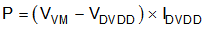
Use Equation 1 to calculate the power dissipated in the device because of the DVDD linear regulator.

Equation 1. GUID-B0987B46-FD31-4841-A714-43A653FFBE75-low.gif

For example, at VVM = 24 V, drawing 20 mA out of DVDD results in a power dissipation as shown in Equation 2.

Equation 2. GUID-7A26F100-A338-4A40-8848-EE3BC7DED61C-low.gif