ZHCSF68D May 2015 – July 2019 DRV8305-Q1
PRODUCTION DATA.
- 1 特性
- 2 应用
- 3 说明
- 4 修订历史记录
- 5 Pin Configuration and Functions
- 6 Specifications
-
7 Detailed Description
- 7.1 Overview
- 7.2 Functional Block Diagram
- 7.3
Feature Description
- 7.3.1 Integrated Three-Phase Gate Driver
- 7.3.2 INHx/INLx: Gate Driver Input Modes
- 7.3.3 VCPH Charge Pump: High-Side Gate Supply
- 7.3.4 VCP_LSD LDO: Low-Side Gate Supply
- 7.3.5 GHx/GLx: Half-Bridge Gate Drivers
- 7.3.6 DVDD and AVDD: Internal Voltage Regulators
- 7.3.7 VREG: Voltage Regulator Output
- 7.3.8 Protection Features
- 7.3.9 Undervoltage Warning (UVFL), Undervoltage Lockout (UVLO), and Overvoltage (OV) Protection
- 7.4 Device Functional Modes
- 7.5 Programming
- 7.6
Register Maps
- 7.6.1 Status Registers
- 7.6.2
Control Registers
- 7.6.2.1 HS Gate Drive Control (Address = 0x5)
- 7.6.2.2 LS Gate Drive Control (Address = 0x6)
- 7.6.2.3 Gate Drive Control (Address = 0x7)
- 7.6.2.4 IC Operation (Address = 0x9)
- 7.6.2.5 Shunt Amplifier Control (Address = 0xA)
- 7.6.2.6 Voltage Regulator Control (Address = 0xB)
- 7.6.2.7 VDS Sense Control (Address = 0xC)
- 8 Application and Implementation
- 9 Power Supply Recommendations
- 10Layout
- 11器件和文档支持
- 12机械、封装和可订购信息
7.3.5.2 Smart Gate Drive Architecture: TDRIVE
The DRV8305-Q1 gate driver uses an integrated state machine (TDRIVE) in the gate driver to protect against excessive current on the gate drive outputs, shoot-through in the external MOSFET, and dV/dt turn on due to switching on the phase nodes. The TDRIVE state machine allows for the design of a robust and efficient motor drive system with minimal overhead.
The state machine incorporates internal handshaking when switching from the low to the high-side external MOSFET or vice-versa. The handshaking is designed to prevent the external MOSFETs from entering a period of cross conduction, also known as shoot-through. The internal handshaking uses the VGS monitors of the DRV8305-Q1 to determine when one MOSFET has been disabled and the other can be enabled. This allows the gate driver to insert an optimized dead time into the system without the risk of cross conduction. Any dead time added externally through the MCU or SPI register will be inserted after the handshake process.
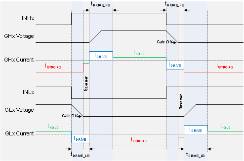
The state machine also incorporates a gate drive timer to ensure that under abnormal circumstances such as a short on the MOSFET gate or the inadvertent turn on of a MOSFET VGS clamp, the high peak current through the DRV8305-Q1 and MOSFET is limited to a fixed duration. This concept is visualized in the figure below. First, the DRV8305-Q1 receives a command to enable or disable the MOSFET through INHx or INLx inputs. Second, the gate driver is enabled and a strong current is applied to the MOSFET gate and the gate voltage begins to change. If the gate voltage has not changed to the desired level after the tDRIVE period (indicating a short circuit or overcurrent condition on the MOSFET gate), the DRV8305-Q1 signals a gate drive fault and the gate drive is disabled to help protect the external MOSFET and DRV8305-Q1. If the MOSFET does successfully enable or disable, after the tDRIVE period the DRV8305-Q1 will enable a lower hold current to ensure the MOSFET remains enabled or disabled and improve efficiency of the gate drive.
Select a tDRIVE time that is longer than the time needed to charge or discharge the gate capacitances of the external MOSFETs. The TDRIVE SPI registers should be configured so that the MOSFET gates are charged completely within tDRIVE during normal operation. If tDRIVE is too low for a given MOSFET, then the MOSFET may not turn on completely. It is suggested to tune these values in-system with the required external MOSFETs to determine the best possible setting for the application. A good starting value is a tDRIVE period that is 2x the expected rise or fall times of the external MOSFET gates. Note that TDRIVE will not increase the PWM time and will simply terminate if a PWM command is received while it is active.
 Figure 11. TDRIVE Gate Drive State Machine