ZHCSF68D May 2015 – July 2019 DRV8305-Q1
PRODUCTION DATA.
- 1 特性
- 2 应用
- 3 说明
- 4 修订历史记录
- 5 Pin Configuration and Functions
- 6 Specifications
-
7 Detailed Description
- 7.1 Overview
- 7.2 Functional Block Diagram
- 7.3
Feature Description
- 7.3.1 Integrated Three-Phase Gate Driver
- 7.3.2 INHx/INLx: Gate Driver Input Modes
- 7.3.3 VCPH Charge Pump: High-Side Gate Supply
- 7.3.4 VCP_LSD LDO: Low-Side Gate Supply
- 7.3.5 GHx/GLx: Half-Bridge Gate Drivers
- 7.3.6 DVDD and AVDD: Internal Voltage Regulators
- 7.3.7 VREG: Voltage Regulator Output
- 7.3.8 Protection Features
- 7.3.9 Undervoltage Warning (UVFL), Undervoltage Lockout (UVLO), and Overvoltage (OV) Protection
- 7.4 Device Functional Modes
- 7.5 Programming
- 7.6
Register Maps
- 7.6.1 Status Registers
- 7.6.2
Control Registers
- 7.6.2.1 HS Gate Drive Control (Address = 0x5)
- 7.6.2.2 LS Gate Drive Control (Address = 0x6)
- 7.6.2.3 Gate Drive Control (Address = 0x7)
- 7.6.2.4 IC Operation (Address = 0x9)
- 7.6.2.5 Shunt Amplifier Control (Address = 0xA)
- 7.6.2.6 Voltage Regulator Control (Address = 0xB)
- 7.6.2.7 VDS Sense Control (Address = 0xC)
- 8 Application and Implementation
- 9 Power Supply Recommendations
- 10Layout
- 11器件和文档支持
- 12机械、封装和可订购信息
7.3.2 INHx/INLx: Gate Driver Input Modes
The DRV8305-Q1 can be operated in three different inputs modes to support various commutation schemes.
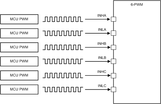
- Table 2 shows the truth table for the 6-PWM input mode. This mode allows for each half-bridge to be placed in one of three states, either High, Low, or Hi-Z, based on the inputs.
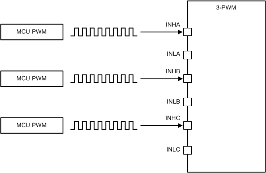
- Table 3 shows the truth table for the 3-PWM input mode. This mode allows for each half-bridge to be placed in one of two states, either High or Low, based on the inputs. The three high-side inputs (INHx) are used to control the state of the half-bridge with the complimentary low-side signals being generated internally. Dead time can be adjusted through the internal setting (DEAD_TIME) in the SPI registers. In this mode all activity on INLx is ignored.
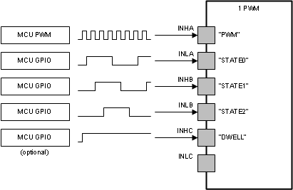
- Table 4 and Table 5 show the truth tables for the 1-PWM input mode. The 1-PWM mode uses an internally stored 6-step block commutation table to control the outputs of the three half-bridge drivers based on one PWM and three GPIO inputs. This mode allows the use of a lower cost microcontroller by requiring only one PWM resource. The PWM signal is applied on pin INHA (PWM_IN) to set the duty cycle of the half-bridge outputs along with the three GPIO signals on pins INLA (PHC_0), INHB (PHC_1), INLB (PHC_2) that serve to set the value of a three bit register for the commutation table. The PWM may be operated from 0-100% duty cycle. The three bit register is used to select the state for each half-bridge for a total of eight states including an align and stop state.
Table 2. 6-PWM Truth Table
| INHx | INLx | GHx | GLx |
|---|---|---|---|
| 1 | 1 | L | L |
| 1 | 0 | H | L |
| 0 | 1 | L | H |
| 0 | 0 | L | L |
 Figure 6. 6-PWM Mode
 Table 3. 3-PWM Truth Table
| INHx | INLx | GHx | GLx |
|---|---|---|---|
| 1 | X | H | L |
| 0 | X | L | H |
 Figure 7. 3-PWM Mode
 An additional and optional GPIO, INHC (DWELL) can be used to facilitate the insertion of dwell states or phase current overlap states between the six commutation steps. This may be used to reduce acoustic noise and improve motion through the reduction of abrupt current direction changes when switching between states. INHC must be high when the state is changed and the dwell state will exist until INHC is taken low. If the dwell states are not being used, the INHC pin can be tied low.
In 1-PWM mode all activity on INLC is ignored.
 Figure 8. 1-PWM Mode
 The method of freewheeling can be selected through an SPI register (COMM_OPTION). Diode freewheeling is when the phase current is carried by the body diode of the external power MOSFET during periods when the MOSFET is reverse biased (current moving from source to drain). In active freewheeling, the power MOSFET is enabled during periods when the MOSFET is reverse biased. This allows the system to improve efficiency due to the typically lower impedance of the MOSFET conduction channel as compared to the body diode. Table 4 shows the truth table for active freewheeling. Table 5) shows the truth table for diode freewheeling.
Table 4. 1-PWM Active Freewheeling
| STATE | INLA:INHB:INLB:INHC | GHA | GLA | GHB | GLB | GHC | GLC |
|---|---|---|---|---|---|---|---|
| AB | 0110 | PWM | !PWM | LOW | HIGH | LOW | LOW |
| AB_CB | 0101 | PWM | !PWM | LOW | HIGH | PWM | !PWM |
| CB | 0100 | LOW | LOW | LOW | HIGH | PWM | !PWM |
| CB_CA | 1101 | LOW | HIGH | LOW | HIGH | PWM | !PWM |
| CA | 1100 | LOW | HIGH | LOW | LOW | PWM | !PWM |
| CA_BA | 1001 | LOW | HIGH | PWM | !PWM | PWM | !PWM |
| BA | 1000 | LOW | HIGH | PWM | !PWM | LOW | LOW |
| BA_BC | 1011 | LOW | HIGH | PWM | !PWM | LOW | HIGH |
| BC | 1010 | LOW | LOW | PWM | !PWM | LOW | HIGH |
| BC_AC | 0011 | PWM | !PWM | PWM | !PWM | LOW | HIGH |
| AC | 0010 | PWM | !PWM | LOW | LOW | LOW | HIGH |
| AC_AB | 0111 | PWM | !PWM | LOW | HIGH | LOW | HIGH |
| Align | 1110 | PWM | !PWM | LOW | HIGH | LOW | HIGH |
| Stop | 0000 | LOW | LOW | LOW | LOW | LOW | LOW |
Table 5. 1-PWM Diode Freewheeling
| STATE | INLA:INHB:INLB:INHC | GHA | GLA | GHB | GLB | GHC | GLC |
|---|---|---|---|---|---|---|---|
| AB | 0110 | PWM | LOW | LOW | HIGH | LOW | LOW |
| AB_CB | 0101 | PWM | LOW | LOW | HIGH | PWM | LOW |
| CB | 0100 | LOW | LOW | LOW | HIGH | PWM | LOW |
| CB_CA | 1101 | LOW | HIGH | LOW | HIGH | PWM | LOW |
| CA | 1100 | LOW | HIGH | LOW | LOW | PWM | LOW |
| CA_BA | 1001 | LOW | HIGH | PWM | LOW | PWM | LOW |
| BA | 1000 | LOW | HIGH | PWM | LOW | LOW | LOW |
| BA_BC | 1011 | LOW | HIGH | PWM | LOW | LOW | HIGH |
| BC | 1010 | LOW | LOW | PWM | LOW | LOW | HIGH |
| BC_AC | 0011 | PWM | LOW | PWM | LOW | LOW | HIGH |
| AC | 0010 | PWM | LOW | LOW | LOW | LOW | HIGH |
| AC_AB | 0111 | PWM | LOW | LOW | HIGH | LOW | HIGH |
| Align | 1110 | PWM | LOW | LOW | HIGH | LOW | HIGH |
| Stop | 0000 | LOW | LOW | LOW | LOW | LOW | LOW |