ZHCSF68D May 2015 – July 2019 DRV8305-Q1
PRODUCTION DATA.
- 1 特性
- 2 应用
- 3 说明
- 4 修订历史记录
- 5 Pin Configuration and Functions
- 6 Specifications
-
7 Detailed Description
- 7.1 Overview
- 7.2 Functional Block Diagram
- 7.3
Feature Description
- 7.3.1 Integrated Three-Phase Gate Driver
- 7.3.2 INHx/INLx: Gate Driver Input Modes
- 7.3.3 VCPH Charge Pump: High-Side Gate Supply
- 7.3.4 VCP_LSD LDO: Low-Side Gate Supply
- 7.3.5 GHx/GLx: Half-Bridge Gate Drivers
- 7.3.6 DVDD and AVDD: Internal Voltage Regulators
- 7.3.7 VREG: Voltage Regulator Output
- 7.3.8 Protection Features
- 7.3.9 Undervoltage Warning (UVFL), Undervoltage Lockout (UVLO), and Overvoltage (OV) Protection
- 7.4 Device Functional Modes
- 7.5 Programming
- 7.6
Register Maps
- 7.6.1 Status Registers
- 7.6.2
Control Registers
- 7.6.2.1 HS Gate Drive Control (Address = 0x5)
- 7.6.2.2 LS Gate Drive Control (Address = 0x6)
- 7.6.2.3 Gate Drive Control (Address = 0x7)
- 7.6.2.4 IC Operation (Address = 0x9)
- 7.6.2.5 Shunt Amplifier Control (Address = 0xA)
- 7.6.2.6 Voltage Regulator Control (Address = 0xB)
- 7.6.2.7 VDS Sense Control (Address = 0xC)
- 8 Application and Implementation
- 9 Power Supply Recommendations
- 10Layout
- 11器件和文档支持
- 12机械、封装和可订购信息
7.3.5.1 Smart Gate Drive Architecture: IDRIVE
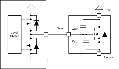
The first component of the gate drive architecture implements adjustable current control for the gates of the external power MOSFETs. This feature allows the gate driver to control the VDS slew rate of the MOSFETs by adjusting the gate drive current. This is realized internally to reduce the need for external components inline with the gates of the MOSFETs. The DRV8305-Q1 provides 12 adjustable source and sink current levels for the high-side (the high-sides of all three phases share the same setting) and low-side gate drivers (the low-sides of all three phases share the same settings). The gate drive levels are adjustable through the SPI registers in both the standby and operating states. This flexibility allows the system designer to tune the performance of the driver for different operating conditions through software alone.
The gate drivers are implemented as temperature compensated, constant current sources up to the 80-mA (sink)/70-mA (source) current settings in order to maintain the accuracy required for precise slew rate control. The current source architecture helps eliminate the temperature, process, and load-dependent variation associated with internal and external series limiting resistors. Beyond that, internal switches are adjusted to create the desired settings up to the 1.25-A (sink)/1-A (source) settings. For higher currents, internal series switches are used to minimize the power losses associated with mirroring such large currents.
Control of the gate current during the MOSFET Miller region is a key component for adjusting the MOSFET VDS rise and fall times. MOSFET VDS slew rates are a critical parameter for optimizing emitted radiations, energy and duration of diode recovery spikes, dV/dt related turn on leading to shoot-through, and voltage transients related to parasitics.
When a MOSFET is enhanced, three different charges must be supplied to the MOSFET gate. The MOSFET drain to source voltage will slew primarily during the Miller region. By controlling the rate of charge to the MOSFET gate (gate drive current strength) during the Miller region, it is possible to optimize the VDS slew rate for the reasons mentioned.
- QGS = Gate-to-source charge
- QGD = Gate-to-drain charge (Miller charge)
- Remaining QG
 Figure 10. MOSFET Charge Example