ZHCSQZ4A July 2022 – October 2022 DRV8300U
PRODUCTION DATA
- 1 特性
- 2 应用
- 3 说明
- 4 Revision History
- 5 Device Comparison Table
- 6 Pin Configuration and Functions
- 7 Specifications
- 8 Detailed Description
- 9 Application and Implementation
- 10Power Supply Recommendations
- 11Layout
- 12Device and Documentation Support
- 13Mechanical, Packaging, and Orderable Information
封装选项
机械数据 (封装 | 引脚)
散热焊盘机械数据 (封装 | 引脚)
- RGE|24
订购信息
6 Pin Configuration and Functions
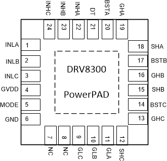
 Figure 6-1 DRV8300UD RGE Package24-Pin VQFN With Exposed Thermal PadTop View
Table 6-1 Pin Functions—24-Pin DRV8300U Devices
| PIN | TYPE(1) | DESCRIPTION | ||
|---|---|---|---|---|
| NAME | NO. | |||
| BSTA | 20 | O | Bootstrap output pin. Connect capacitor between BSTA and SHA | |
| BSTB | 17 | O | Bootstrap output pin. Connect capacitor between BSTB and SHB | |
| BSTC | 14 | O | Bootstrap output pin. Connect capacitor between BSTC and SHC | |
| DT | 21 | I | Deadtime input pin. Connect resistor to ground for variable deadtime, fixed deadtime when left it floating | |
| GHA | 19 | O | High-side gate driver output. Connect to the gate of the high-side power MOSFET. | |
| GHB | 16 | O | High-side gate driver output. Connect to the gate of the high-side power MOSFET. | |
| GHC | 13 | O | High-side gate driver output. Connect to the gate of the high-side power MOSFET. | |
| GLA | 11 | O | Low-side gate driver output. Connect to the gate of the low-side power MOSFET. | |
| GLB | 10 | O | Low-side gate driver output. Connect to the gate of the low-side power MOSFET. | |
| GLC | 9 | O | Low-side gate driver output. Connect to the gate of the low-side power MOSFET. | |
| INHA | 22 | I | High-side gate driver control input. This pin controls the output of the high-side gate driver. | |
| INHB | 23 | I | High-side gate driver control input. This pin controls the output of the high-side gate driver. | |
| INHC | 24 | I | High-side gate driver control input. This pin controls the output of the high-side gate driver. | |
| INLA | 1 | I | Low-side gate driver control input. This pin controls the output of the low-side gate driver. | |
| INLB | 2 | I | Low-side gate driver control input. This pin controls the output of the low-side gate driver. | |
| INLC | 3 | I | Low-side gate driver control input. This pin controls the output of the low-side gate driver. | |
| MODE | 5 | I | Mode Input controls polarity of GLx compared to INLx inputs. Mode pin floating: GLx output polarity same(Non-Inverted) as INLx input Mode pin to GVDD: GLx output polarity inverted compared to INLx input | |
| NC | 7, 8 | NC | No internal connection. This pin can be left floating or connected to system ground. | |
| GND | 6 | PWR | Device ground. | |
| SHA | 18 | I | High-side source sense input. Connect to the high-side power MOSFET source. | |
| SHB | 15 | I | High-side source sense input. Connect to the high-side power MOSFET source. | |
| SHC | 12 | I | High-side source sense input. Connect to the high-side power MOSFET source. | |
| GVDD | 4 | PWR | Gate driver power supply input. Connect a X5R or X7R, GVDD-rated ceramic and greater then or equal to 10-uF local capacitance between the GVDD and GND pins. | |
(1) PWR = power, I = input, O = output, NC = no connection
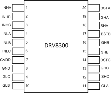
 Figure 6-2 DRV8300UD, DRV8300UDI PW Package20-Pin TSSOPTop View
Table 6-2 Pin Functions—20-Pin DRV8300U Devices
| PIN | TYPE1 | DESCRIPTION | ||
|---|---|---|---|---|
| NAME | NO. | |||
| BSTA | 20 | O | Bootstrap output pin. Connect capacitor between BSTA and SHA | |
| BSTB | 17 | O | Bootstrap output pin. Connect capacitor between BSTB and SHB | |
| BSTC | 14 | O | Bootstrap output pin. Connect capacitor between BSTC and SHC | |
| GHA | 19 | O | High-side gate driver output. Connect to the gate of the high-side power MOSFET. | |
| GHB | 16 | O | High-side gate driver output. Connect to the gate of the high-side power MOSFET. | |
| GHC | 13 | O | High-side gate driver output. Connect to the gate of the high-side power MOSFET. | |
| GLA | 11 | O | Low-side gate driver output. Connect to the gate of the low-side power MOSFET. | |
| GLB | 10 | O | Low-side gate driver output. Connect to the gate of the low-side power MOSFET. | |
| GLC | 9 | O | Low-side gate driver output. Connect to the gate of the low-side power MOSFET. | |
| INHA | 1 | I | High-side gate driver control input. This pin controls the output of the high-side gate driver. | |
| INHB | 2 | I | High-side gate driver control input. This pin controls the output of the high-side gate driver. | |
| INHC | 3 | I | High-side gate driver control input. This pin controls the output of the high-side gate driver. | |
| INLA | 4 | I | Low-side gate driver control input. This pin controls the output of the low-side gate driver. | |
| INLB | 5 | I | Low-side gate driver control input. This pin controls the output of the low-side gate driver. | |
| INLC | 6 | I | Low-side gate driver control input. This pin controls the output of the low-side gate driver. | |
| GND | 8 | PWR | Device ground. | |
| SHA | 18 | I | High-side source sense input. Connect to the high-side power MOSFET source. | |
| SHB | 15 | I | High-side source sense input. Connect to the high-side power MOSFET source. | |
| SHC | 12 | I | High-side source sense input. Connect to the high-side power MOSFET source. | |
| GVDD | 7 | PWR | Gate driver power supply input. Connect a X5R or X7R, GVDD-rated ceramic and greater then or equal to 10-uF local capacitance between the GVDD and GND pins. | |
- PWR = power, I = input, O = output, NC = no connection