ZHCSQZ4A July 2022 – October 2022 DRV8300U
PRODUCTION DATA
- 1 特性
- 2 应用
- 3 说明
- 4 Revision History
- 5 Device Comparison Table
- 6 Pin Configuration and Functions
- 7 Specifications
- 8 Detailed Description
- 9 Application and Implementation
- 10Power Supply Recommendations
- 11Layout
- 12Device and Documentation Support
- 13Mechanical, Packaging, and Orderable Information
封装选项
机械数据 (封装 | 引脚)
散热焊盘机械数据 (封装 | 引脚)
- RGE|24
订购信息
8.3.1.2 Mode (Inverting and non inverting INLx)
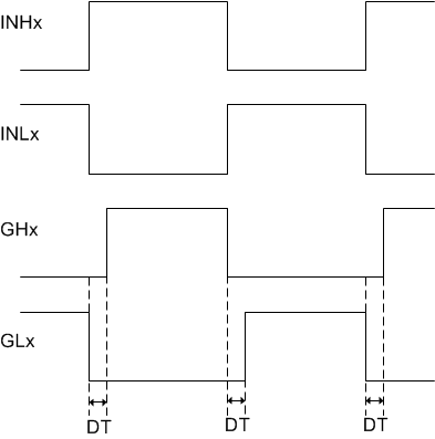
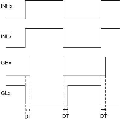
The DRV8300U has flexibility of accepting different kind of inputs on INLx. In the devices with MODE pin (QFN package), the DRV8300U provides option of configuring the GLx outputs to be inverted or non-inverted compared to polarity of signal on INLx pins. When the MODE pin is left floating, the INLx is configured to be in non-inverting mode and GLx output is in phase with respect to INLx (see Figure 8-3), whereas when the MODE pin is connected to GVDD, GLx output is out of phase with respect to INLx (see Figure 8-4). In devices without MODE pin (TSSOP package device), there are different device option available for inverting and non inverting inputs (see Section 5).
 Figure 8-3 Non-Inverted INLx inputs
 Figure 8-4 Inverted INLx inputs