ZHCSK74A August   2019  – April 2020 DRV425-Q1

PRODUCTION DATA.  

  1. 特性
  2. 应用
  3. 说明
    1.     Device Images
      1.      简化原理图
  4. 修订历史记录
  5. Pin Configuration and Functions
    1.     Pin Functions
  6. Specifications
    1. 6.1 Absolute Maximum Ratings
    2. 6.2 ESD Ratings
    3. 6.3 Recommended Operating Conditions
    4. 6.4 Thermal Information
    5. 6.5 Electrical Characteristics
    6. 6.6 Typical Characteristics
  7. Detailed Description
    1. 7.1 Overview
    2. 7.2 Functional Block Diagram
    3. 7.3 Feature Description
      1. 7.3.1 Fluxgate Sensor Front-End
        1. 7.3.1.1 Fluxgate Sensor
        2. 7.3.1.2 Bandwidth
        3. 7.3.1.3 Differential Driver for the Internal Compensation Coil
        4. 7.3.1.4 Magnetic Field Range, Overrange Indicator, and Error Flag
      2. 7.3.2 Shunt-Sense Amplifier
      3. 7.3.3 Voltage Reference
      4. 7.3.4 Low-Power Operation
    4. 7.4 Device Functional Modes
  8. Application and Implementation
    1. 8.1 Application Information
    2. 8.2 Typical Applications
      1. 8.2.1 Linear Position Sensing
        1. 8.2.1.1 Design Requirements
        2. 8.2.1.2 Detailed Design Procedure
        3. 8.2.1.3 Application Curves
      2. 8.2.2 Current Sensing in Busbars
        1. 8.2.2.1 Design Requirements
        2. 8.2.2.2 Detailed Design Procedure
        3. 8.2.2.3 Application Curves
  9. Power Supply Recommendations
    1. 9.1 Power Supply Decoupling
    2. 9.2 Power-On Start-Up and Brownout
    3. 9.3 Power Dissipation
      1. 9.3.1 Thermal Pad
  10. 10Layout
    1. 10.1 Layout Guidelines
    2. 10.2 Layout Example
  11. 11器件和文档支持
    1. 11.1 文档支持
      1. 11.1.1 相关文档
    2. 11.2 接收文档更新通知
    3. 11.3 支持资源
    4. 11.4 商标
    5. 11.5 静电放电警告
    6. 11.6 Glossary
  12. 12机械、封装和可订购信息

封装选项

机械数据 (封装 | 引脚)
散热焊盘机械数据 (封装 | 引脚)
订购信息

Application Curves

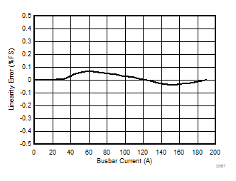
Figure 74 and Figure 75 show the measurement results on a 16-mm wide and 6-mm thick copper busbar with a 12-mm hole diameter using the circuit shown in Figure 73. The two DRV425-Q1 devices are placed at a distance of 1 mm from each other on opposite sides of the PCB. The measurement range is ±500 A; measurement results are limited by test setup. Independent operation of the two DRV425-Q1 sensors increases the measurement range to ±1000 A with the same busbar geometry.
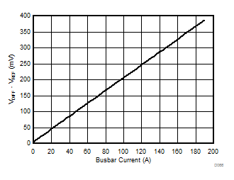
DRV425-Q1 D066_SBOS729.gif
Figure 74. Analog Output Voltage vs
Busbar Current
DRV425-Q1 D067_SBOS729.gif
Figure 75. Linearity Error vs Busbar Current