ZHCSHA0E January 2018 – March 2021 DRV10974
PRODUCTION DATA
- 1 特性
- 2 应用
- 3 说明
- 4 Revision History
- 5 Pin Configuration and Functions
- 6 Specifications
-
7 Detailed Description
- 7.1 Overview
- 7.2 Functional Block Diagram
- 7.3 Feature Description
- 7.4 Device Functional Modes
- 8 Application and Implementation
- 9 Power Supply Recommendations
- 10Layout
- 11Device and Documentation Support
- 12Mechanical, Packaging, and Orderable Information
封装选项
机械数据 (封装 | 引脚)
散热焊盘机械数据 (封装 | 引脚)
订购信息
7.3.1 Speed Input and Control
The DRV10974 device has a three-phase 25-kHz PWM (fPWM_OUT) output that has an average value of sinusoidal waveforms from phase to phase as shown in #T4509467-24. When any phase is measured with reference to ground, the waveform observed is a PWM-encoded sinusoid coupled with third-order harmonics as shown in #T4509467-25. This encoding scheme simplifies the driver requirements because one phase output is always equal to zero.
 Figure 7-2 Sinusoidal Voltage
 Figure 7-3 PWM Encoded Phase Output and the Average Value
The output amplitude is determined by the supply voltage (VCC) and the PWM-commanded duty cycle (PWM) as calculated in #T4509467-57 and shown in #T4509467-27. The maximum amplitude is applied when the commanded PWM duty cycle is slightly less than 100% in order to keep the 25-kHz PWM rate (fPWM_OUT).
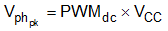
 Figure 7-4 Output Voltage Amplitude Adjustment
The motor speed is controlled indirectly by using the PWM command to control the amplitude of the phase voltages which are applied to the motor. The PWM pin can be driven by either a digital duty cycle or an analog voltage.
The duty cycle of the PWM input (PWM) is passed through a low-pass filter that ramps from 0% to 100% duty cycle in 120 ms. The control resolution is approximately 0.2% (DCSTEP). The signal path from PWM input to PWM motor is shown in #T4509467-28.
 Figure 7-5 PWM Command Input Control Diagram
The output peak amplitude is described by #T4509467-57 when PWMdc > 15% (the minimum-operation duty cycle). When the PWM-commanded duty cycle is lower than the minimum-operation duty cycle and higher than 1.5% (DCON_MIN), the output is controlled the by the minimum-operation duty cycle (DCMIN). This is shown in #X2591 for analog input, and for duty cycles greater than 1.5% (DCON_MIN) for digital input. If the supply voltage (VVCC) > 14 V, the maximum PWMdc is limited to 14 V / VVCC.
 Figure 7-6 PWM-Mode Speed-Control Transfer Function
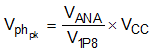
When the PWM pin is driven with an analog voltage, the output peak amplitude depends on the supply voltage, the analog voltage on the PWM pin (VANA), and the voltage of V1P8 (VV1P8). This is shown in #SLVSDN21017:
Note the output peak amplitude is described by #SLVSDN21017 when the VANA > 0.27 V or 15% of 1.8 V. This is the equivalent of the minimum-operation duty cycle percentage of 15% (DCMIN). When the analog voltage on the PWM pin is lower than the minimum-operation duty-cycle percentage but higher than the zero-speed analog voltage (VANA_ZS), the output is controlled by the minimum-operation duty cycle. When the analog voltage on the PWM pin is below zero-speed analog voltage, the DRV10974 enters low-power mode. This is shown in #SLVSDN21018.
 Figure 7-7 Analog-Mode Speed-Control Transfer Function