ZHCSOV8A October   2021  – January 2022 DLPC3420

PRODUCTION DATA  

  1. 特性
  2. 应用
  3. 说明
  4. Revision History
  5. Pin Configuration and Functions
  6. Specifications
    1. 6.1  Absolute Maximum Ratings
    2. 6.2  ESD Ratings
    3. 6.3  Recommended Operating Conditions
    4. 6.4  Thermal Information
    5. 6.5  Power Electrical Characteristics
    6. 6.6  Pin Electrical Characteristics
    7. 6.7  Internal Pullup and Pulldown Electrical Characteristics
    8. 6.8  DMD Sub-LVDS Interface Electrical Characteristics
    9. 6.9  DMD Low-Speed Interface Electrical Characteristics
    10. 6.10 System Oscillator Timing Requirements
    11. 6.11 Power Supply and Reset Timing Requirements
    12. 6.12 Parallel Interface Frame Timing Requirements
    13. 6.13 Parallel Interface General Timing Requirements
    14. 6.14 BT656 Interface General Timing Requirements
    15. 6.15 DSI Host Timing Requirements
    16. 6.16 Flash Interface Timing Requirements
    17. 6.17 Other Timing Requirements
    18. 6.18 DMD Sub-LVDS Interface Switching Characteristics
    19. 6.19 DMD Parking Switching Characteristics
    20. 6.20 Chipset Component Usage Specification
  7. Detailed Description
    1. 7.1 Overview
    2. 7.2 Functional Block Diagram
    3. 7.3 Feature Description
      1. 7.3.1 Input Source Requirements
        1. 7.3.1.1 Supported Resolution and Frame Rates
        2. 7.3.1.2 Parallel Interface
          1. 7.3.1.2.1 PDATA Bus – Parallel Interface Bit Mapping Modes
        3. 7.3.1.3 DSI Interface
      2. 7.3.2 Device Startup
      3. 7.3.3 SPI Flash
        1. 7.3.3.1 SPI Flash Interface
        2. 7.3.3.2 SPI Flash Programming
      4. 7.3.4 I2C Interface
      5. 7.3.5 Content Adaptive Illumination Control (CAIC)
      6. 7.3.6 Test Point Support
      7. 7.3.7 DMD Interface
        1. 7.3.7.1 Sub-LVDS (HS) Interface
    4. 7.4 Device Functional Modes
    5. 7.5 Programming
  8. Application and Implementation
    1. 8.1 Application Information
    2. 8.2 Typical Application
      1. 8.2.1 Design Requirements
      2. 8.2.2 Detailed Design Procedure
      3. 8.2.3 Application Curve
  9. Power Supply Recommendations
    1. 9.1 PLL Design Considerations
    2. 9.2 System Power-Up and Power-Down Sequence
    3. 9.3 Power-Up Initialization Sequence
    4. 9.4 DMD Fast Park Control (PARKZ)
    5. 9.5 Hot Plug I/O Usage
  10. 10Layout
    1. 10.1 Layout Guidelines
      1. 10.1.1  PLL Power Layout
      2. 10.1.2  Reference Clock Layout
        1. 10.1.2.1 Recommended Crystal Oscillator Configuration
      3. 10.1.3  DSI Interface Layout
      4. 10.1.4  Unused Pins
      5. 10.1.5  DMD Control and Sub-LVDS Signals
      6. 10.1.6  Layer Changes
      7. 10.1.7  Stubs
      8. 10.1.8  Terminations
      9. 10.1.9  Routing Vias
      10. 10.1.10 Thermal Considerations
    2. 10.2 Layout Example
  11. 11Device and Documentation Support
    1. 11.1 Device Support
      1. 11.1.1 第三方产品免责声明
      2. 11.1.2 Device Nomenclature
        1. 11.1.2.1 Device Markings
      3. 11.1.3 Video Timing Parameter Definitions
    2. 11.2 Related Documentation
    3. 11.3 Related Links
    4. 11.4 接收文档更新通知
    5. 11.5 支持资源
    6. 11.6 Trademarks
    7. 11.7 Electrostatic Discharge Caution
    8. 11.8 术语表
  12. 12Mechanical, Packaging, and Orderable Information
  13. 13Package Option Addendum
    1. 13.1 Packaging Information

封装选项

机械数据 (封装 | 引脚)
散热焊盘机械数据 (封装 | 引脚)

Device Markings

GUID-20210927-SS0I-ZJPK-LMTG-6CCKGKK0CLWS-low.gif

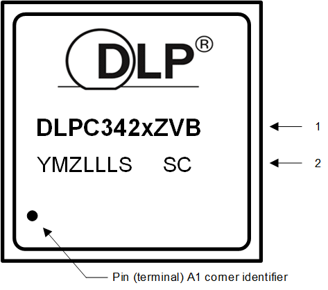
Marking Definitions:

Line 1:DLP Device Name: DLPC342x where x is a "0" for this device
Line 2:YMZLLLS SC: Foundry lot code for semiconductor wafers and lead-free solder ball marking
YM: Year Month
Z, S: Assembly site
LLL: Assembly lot traceability
SC: Solder ball composition
   e1: Indicates lead-free solder balls consisting of SnAgCu
   G8: Indicates lead-free solder balls consisting of tin-silver-copper (SnAgCu) with silver content
   less than or equal to 1.5% and that the mold compound meets TI's definition of green
Note:

  1. Engineering prototype samples are marked with an X suffix appended to the TI part number. For example, 2512737-0001X.
  2. See Section 7.3.1.1, for DLPC342x resolutions on the DMD supported per part number.