ZHCSE88A October 2015 – February 2023 DLPA3005
PRODUCTION DATA
- 1 特性
- 2 应用
- 3 说明
- 4 Revision History
- 5 Pin Configuration and Functions
- 6 Specifications
-
7 Detailed Description
- 7.1 Overview
- 7.2 Functional Block Description
- 7.3
Feature Description
- 7.3.1 Supply and Monitoring
- 7.3.2 Illumination
- 7.3.3 External Power FET Selection
- 7.3.4 DMD Supplies
- 7.3.5 Buck Converters
- 7.3.6 Auxiliary LDOs
- 7.3.7 Measurement System
- 7.4 Device Functional Modes
- 7.5 Programming
- 7.6 Register Maps
- 8 Application and Implementation
- 9 Power Supply Recommendations
- 10Layout
- 11Device and Documentation Support
- 12Mechanical, Packaging, and Orderable Information
8.2.2 Detailed Design Procedure
To connect the 0.47 1080 DMD (DLP4710), two DLPC3439s, and DLPA3005, see the reference design schematic. When a circuit board layout is created from this schematic a very small circuit board is possible. An example small board layout is included in the reference design data base. Layout guidelines should be followed to achieve reliable projector operation. The optical engine that has the LED packages and the DMD mounted to it is typically supplied by an optical OEM who specializes in designing optics for DLP projectors.
The component selection of the buck converter is mainly determined by the output voltage. #GUID-D8112734-2CAE-4383-A2EB-40C2F1B920C4/DLPS0418928 shows the recommended value for inductor LOUT and capacitor COUT for a given output voltage.
| VOUT (V) | LOUT (µH) | COUT (µF) | |||
|---|---|---|---|---|---|
| MIN | TYP | MAX | MIN | MAX | |
| 1 – 1.5 | 1.5 | 2.2 | 4.7 | 22 | 68 |
| 1.5 – 3.3 | 2.2 | 3.3 | 4.7 | 22 | 68 |
| 3.3 – 5 | 3.3 | 4.7 | 22 | 68 | |
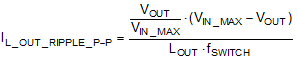
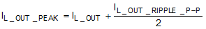
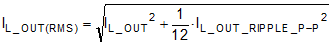
The inductor peak-to-peak ripple current, peak current and RMS current can be calculated using Equation 8, Equation 9 and Equation 10 respectively. The inductor saturation current rating must be greater than the calculated peak current. Likewise, the RMS or heating current rating of the inductor must be greater than the calculated RMS current. The switching frequency of the buck converter is approximately 600 kHz (ƒSWITCH).
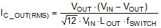
The capacitor value and ESR determines the level of output voltage ripple. The buck converter is intended for use with ceramic or other low ESR capacitors. Recommended values range from 22 to 68 μF. Equation 11 can be used to determine the required RMS current rating for the output capacitor.
Two other components need to be selected in the buck converter configuration. The value of the input-capacitor (pin PWRx_VIN) should be equal or greater than halve the selected output capacitance COUT. In this case CIN 2 × 10 µF is sufficient. The capacitor between PWRx_SWITCH and PWRx_BOOST is a charge pump capacitor to drive the high side FET. The recommended value is 100 nF.
Since the switching edges of the buck converter are relatively fast, voltage overshoot and ringing can become a problem. To overcome this problem a snubber network is used. The snubber circuit consists of a resistor and capacitor that are connected in series from the switch node to ground. The snubber circuit is used to damp the parasitic inductances and capacitances during the switching transitions. This circuit reduces the ringing voltage and also reduces the number of ringing cycles. The snubber network is formed by RSNx and CSNx. More information on controlling switch-node ringing in synchronous buck converters and configuring the snubber can be found in Analog Applications Journal.