ZHCSE88A October 2015 – February 2023 DLPA3005
PRODUCTION DATA
- 1 特性
- 2 应用
- 3 说明
- 4 Revision History
- 5 Pin Configuration and Functions
- 6 Specifications
-
7 Detailed Description
- 7.1 Overview
- 7.2 Functional Block Description
- 7.3
Feature Description
- 7.3.1 Supply and Monitoring
- 7.3.2 Illumination
- 7.3.3 External Power FET Selection
- 7.3.4 DMD Supplies
- 7.3.5 Buck Converters
- 7.3.6 Auxiliary LDOs
- 7.3.7 Measurement System
- 7.4 Device Functional Modes
- 7.5 Programming
- 7.6 Register Maps
- 8 Application and Implementation
- 9 Power Supply Recommendations
- 10Layout
- 11Device and Documentation Support
- 12Mechanical, Packaging, and Orderable Information
7.3.2.3 Illumination Driver A
The illumination driver of the DLPA3005 is a buck controller for driving two external low-ohmic N-channel FETs (#DLPS0559754). The theory of operation of a buck converter is explained in the application note Understanding Buck Power Stages in Switchmode Power Supplies. For proper operation, selection of the external components is very important, especially the inductor LOUT and the output capacitor COUT. For best efficiency and ripple performance, an inductor and capacitor should be chosen with low equivalent series resistance (ESR).
 Figure 7-4 Typical Illumination Driver Configuration
Several factors determine the component selection of the buck converter, such as input voltage (SYSPWR), desired output voltage (VLED) and the allowed output current ripple. Configuration starts with selecting the inductor LOUT.
The value of the inductance of a buck power stage is selected such that the peak-to-peak ripple current flowing in the inductor stays within a certain range. Here, the target is set to have an inductor current ripple, kI_RIPPLE, less than 0.3 (30%). The minimum inductor value can be calculated given the input and output voltage, output current, switching frequency of the buck converter (ƒSWITCH= 600 kHz), and inductor ripple of 0.3 (30%):
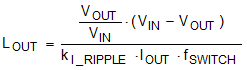
Example: VIN= 12 V, VOUT= 4.3 V, IOUT= 16 A results in an inductor value of LOUT= 1 µH
Once the inductor is selected, the output capacitor COUT can be determined. The value is calculated using the fact that the frequency compensation of the illumination loop has been designed for an LC-tank resonance frequency of 15 kHz:
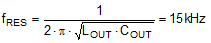
Example: COUT= 110 µF given that LOUT= 1 µH. A practical value is 2 × 68 µF. Here, a parallel connection of two capacitors is chosen to lower the ESR even further.
The selected inductor and capacitor determine the output voltage ripple. The resulting output voltage ripple VLED_RIPPLE is a function of the inductor ripple kI_RIPPLE, output current IOUT, switching frequency ƒSWITCH and the capacitor value COUT:
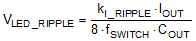
Example: kI_RIPPLE= 0.3, IOUT= 16 A, ƒSWITCH= 600 kHz and COUT= 2 x 68 µF results in an output voltage ripple of VLED_RIPPLE= 7 mVpp
As can be seen, this is a relatively small ripple.
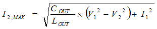
It is strongly advised to keep the capacitance value low. The larger the capacitor value the more energy is stored. In case of a VLED going down stored energy needs to be dissipated. This might result in a large discharge current. For a VLED step down from V1 to V2, while the LED current was I1. The theoretical peak reverse current is:
Depending on the selected external FETs, the following three components might need to be added for each power FET:
- Gate series resistor (RG)
- Gate series diode (DG)
- Gate parallel capacitance (CG)
It is advisable to have placeholders for these components in the board design.
The gate series resistors can be used to slow down the enable transient of the power FET. Since large currents are being switched, a fast transient implies a potential risk on ringing. Slowing down the turn-on transient reduces the edge steepness of the drain current and thus reduces the induced inductive ringing. A resistance of a few Ohm typically is sufficient.
The gate series resistance is also present in the turn-off transient of the power FET. This might have a negative effect on the non-overlap timing. In order to keep the turn-off transient of the power FET fast, a parallel diode with the gate series resistance can be used. The cathode of the diode should be directed to the DLPA3005 device in order have fast gate pull-down.
A third component that might be needed, depending on the specific configuration and FET selection, is an extra gate-source filter capacitance. Specifically, for the higher supply voltages this capacitance is advisable. Due to a large drain voltage swing and the drain-gate capacitance, the gate of a disabled power FET might be pulled high parasitically.
For the low-side FET this can happen at the end of the non-overlap time while the power converter is supplying current. For that case the switch node is low at the end of the non-overlap time. Enabling the high-side FET pulls high the switch node. Due to the large and steep switch node edge, charge is injected through the drain-gate capacitance of the low-side FET into the gate of the low-side FET. As a result the low-side FET can be enabled for a short period of time causing a shoot-through current.
For the high-side FET a dual case exists. If the power converter is discharging VLED, the power converter current is directed inward and thus at the end of the non-overlap time the switch node is high. If at that moment the low-side FET is enabled, via the gate-drain capacitance of the high-side FET charge is being injected into the gate of the high-side FET potentially causing the device to switch on for a short amount of time. That will cause a shoot through current as well.
To reduce the effect of the charge injection through the drain-gate capacitance, an extra gate-source filter capacitance can be used. Assuming a linear voltage division between gate-source capacitance and gate-drain capacitance, for a 20V supply voltage the ratio of gate-source capacitance and gate-drain capacitance should be kept to about 1:10 or larger. It is advised to carefully test the gate-drive signals and the switch node for potential cross conduction.
Sometimes dual FETs are used to spread out power dissipation (heat). To prevent parasitic gate-oscillation a structure, as shown in #DLPS0555586 is suggested. Each gate is being isolated with RISO to damp potential oscillations. A resistance of 1 Ohm is typically sufficient.
 Figure 7-5 Using RISO to Prevent Gate Oscillations When Using Power FETs in Parallel
Finally, two other components need to be selected in the buck converter. The value of the input-capacitor (pin ILLUM_A_VIN) should be equal or greater than the selected output capacitance COUT, in this case ≥2 × 68 µF. The capacitor between ILLUM_A_SWITCH and ILLUM_A_BOOST is a charge pump capacitor to drive the high side FET. The recommended value is 100 nF.