ZHCSOK9A october 2021 – june 2023 DLPA300
PRODUCTION DATA
- 1
- 1 特性
- 2 应用
- 3 说明
- 4 Revision History
- 5 Pin Configuration and Functions
-
6 Specifications
- 6.1 Absolute Maximum Ratings
- 6.2 ESD Ratings
- 6.3 Recommended Operating Conditions
- 6.4 Thermal Information
- 6.5 Electrical Characteristics Control Logic
- 6.6 5-V Linear Regulator
- 6.7 Bias Voltage Boost Converter
- 6.8 Reset Voltage Buck-Boost Converter
- 6.9 VOFFSET Regulator
- 6.10 Switching Characteristics
- 7 Detailed Description
- 8 Application and Implementation
- 9 Power Supply Recommendations
- 10Layout
- 11Device and Documentation Support
- 12Mechanical, Packaging, and Orderable Information
5 Pin Configuration and Functions
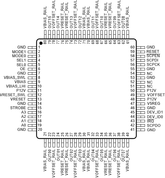
 Figure 5-1 PFP Package80-Pin HTQFPTop View
Table 5-1 Package Pinout
| PIN | I/O (INPUT DEFAULT) |
DESCRIPTION | |
|---|---|---|---|
| NAME | NO. | ||
| OUT00 | 22 | Output | 16 micromirror clocking waveform outputs (enabled by OE = 0) |
| OUT01 | 24 | Output | |
| OUT02 | 27 | Output | |
| OUT03 | 29 | Output | |
| OUT04 | 32 | Output | |
| OUT05 | 34 | Output | |
| OUT06 | 37 | Output | |
| OUT07 | 39 | Output | |
| OUT08 | 62 | Output | |
| OUT09 | 64 | Output | |
| OUT10 | 67 | Output | |
| OUT11 | 69 | Output | |
| OUT12 | 72 | Output | |
| OUT13 | 74 | Output | |
| OUT14 | 77 | Output | |
| OUT15 | 79 | Output | |
| A0 | 19 | Input (pulldown) | Output Address. Used to select which OUTxx pin is active at a given time |
| A1 | 18 | Input (pulldown) | |
| A2 | 17 | Input (pulldown) | |
| A3 | 16 | Input (pulldown) | |
| MODE0 | 3 | Input (pulldown) | Mode Select. Used to determine the operating mode of the DLPA300 |
| MODE1 | 2 | Input (pulldown) | |
| SEL0 | 5 | Input (pulldown) | Output Voltage Select. Used to switch the voltage applied to the addressed OUTxx pin |
| SEL1 | 4 | Input (pulldown) | |
| STROBE | 15 | Input (pulldown) | A rising edge on STROBE latches in the control signals after a tristate delay |
| OE | 6 | Input (pullup) | Asynchronous input
controls whether the 16 OUTxx pins are active or are in a in
high-impedance state. OE = 0 : Enabled. OE = 1 : High Z |
| RESET | 59 | Input (pullup) | Resets the DLPA300 internal logic. Active low. Asynchronous |
| SCPEN | 58 | Input (pullup) | Enables serial bus data transfers. Active low |
| SCPDI | 57 | Input (pull down) | Serial bus data input. Clocked in on the falling edge of SCPCK |
| SCPCK | 56 | Input (pull down) | Serial bus clock. Provided by chipset controller |
| SCPDO | 42 | Output | Serial bus data output (open drain).
Clocked out on the rising edge of SCPCK. A 1-kΩ pullup resistor to the chip-set controller VDD supply is recommended. |
| IRQ | 43 | Output | Interrupt request output to the chipset
Controller. Active low. A 1-kΩ pullup resistor to the chip-set controller VDD supply is recommended. |
| DEV_ID1 | 45 | Input (pullup) |
Serial bus device address: 00 = all; 01 = device 1; 10 = device 2; 11 = device 3 |
| DEV_ID0 | 44 | Input (pullup) | |
| VBIAS | 9 | Output | One of three specialized voltages the DLPA300 generates |
| VBIAS_LHI | 10 | Input | Current limiter output for VBIAS supply (also the VBIAS switching inductor input) |
| VBIAS_SWL | 8 | Input | Connection point for VBIAS supply switching inductor |
| VBIAS_RAIL | 21, 30, 31, 40, 61, 70, 71, 80 | Input | The internally used VBIAS supply rail. Internally isolated from VBIAS |
| VRESET | 13 | No Connect | This pin is unused by the DLPA300. |
| VRESET_SWL | 12 | No Connect | This pin is unused by the DLPA300. |
| VRESET_RAIL(1) | 25, 26, 35,36, 65, 66, 75, 76 | Input | The internally-used VRESET supply rail. Internally isolated from VRESET. The external VRESET supply is connected to this pin. The package thermal pad is tied to this voltage level.(1) |
| VOFFSET | 49 | Output | One of three specialized voltages the DLPA300 generates |
| VOFFSET_RAIL | 23, 28, 33, 38, 63, 68, 73, 78 | Input | The internally-used VOFFSET supply rail. Internally isolated from VOFFSET |
| GND | 1, 7, 14, 20, 41, 46, 53, 55, 60 | GND | Common ground |
| V5REG | 47 | Output | The 5-V logic supply output |
| P12V | 11, 48, 50 | Input | The main power input to the DLPA300 |
| NC | 51, 52, 54 | No Connect | No connect |
(1) Exposed thermal pad is internally connected to VRESET_RAIL.