ZHCSD21 October 2014 DLP6500FLQ
PRODUCTION DATA.
- 1 特性
- 2 应用
- 3 说明
- 4 修订历史记录
- 5 Pin Configuration and Functions
-
6 Specifications
- 6.1 Absolute Maximum Ratings
- 6.2 Handling Ratings
- 6.3 Recommended Operating Conditions
- 6.4 Thermal Information
- 6.5 Electrical Characteristics
- 6.6 Timing Requirements
- 6.7 Typical Characteristics
- 6.8 System Mounting Interface Loads
- 6.9 Micromirror Array Physical Characteristics
- 6.10 Micromirror Array Optical Characteristics
- 6.11 Window Characteristics
- 6.12 Chipset Component Usage Specification
- 7 Detailed Description
- 8 Application and Implementation
- 9 Power Supply Recommendations
- 10Layout
- 11器件和文档支持
- 12机械封装和可订购信息
7 Detailed Description
7.1 Overview
DLP6500FLQ is a 0.65 inch diagonal spatial light modulator which consists of an array of highly reflective aluminum micromirrors. Pixel array size and square grid pixel arrangement are shown in Figure 11.
The DMD is an electrical input, optical output micro-electrical-mechanical system (MEMS). The electrical interface is Low Voltage Differential Signaling (LVDS), Double Data Rate (DDR).
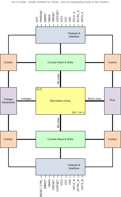
DLP6500FLQ DMD consists of a two-dimensional array of 1-bit CMOS memory cells. The array is organized in a grid of M memory cell columns by N memory cell rows. Refer to the Functional Block Diagram.
The positive or negative deflection angle of the micromirrors can be individually controlled by changing the address voltage of underlying CMOS addressing circuitry and micromirror reset signals (MBRST).
Each cell of the M × N memory array drives its true and complement (‘Q’ and ‘QB’) data to two electrodes underlying one micromirror, one electrode on each side of the diagonal axis of rotation. Refer to Micromirror Array Optical Characteristics. The micromirrors are electrically tied to the micromirror reset signals (MBRST) and the micromirror array is divided into reset groups.
Electrostatic potentials between a micromirror and its memory data electrodes cause the micromirror to tilt toward the illumination source in a DLP projection system or away from it, thus reflecting its incident light into or out of an optical collection aperture. The positive (+) tilt angle state corresponds to an 'on' pixel, and the negative (–) tilt angle state corresponds to an 'off' pixel.
Refer to Micromirror Array Optical Characteristics for the ± tilt angle specifications. Refer to Pin Configuration and Functions for more information on micromirror reset control.
7.2 Functional Block Diagram
7.3 Feature Description
DLP6500FLQ device consists of highly reflective, digitally switchable, micrometer-sized mirrors (micromirrors) organized in a two-dimensional orthogonal pixel array. Refer to Figure 11 and Figure 13.
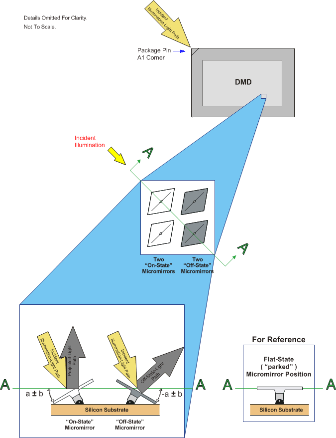
Each aluminum micromirror is switchable between two discrete angular positions, –α and +α. The angular positions are measured relative to the micromirror array plane, which is parallel to the silicon substrate. Refer to Micromirror Array Optical Characteristics and Figure 14.
The parked position of the micromirror is not a latched position and is therefore not necessarily perfectly parallel to the array plane. Individual micromirror flat state angular positions may vary. Tilt direction of the micromirror is perpendicular to the hinge-axis. The on-state landed position is directed toward the left-top edge of the package, as shown in Figure 13.
Each individual micromirror is positioned over a corresponding CMOS memory cell. The angular position of a specific micromirror is determined by the binary state (logic 0 or 1) of the corresponding CMOS memory cell contents, after the mirror clocking pulse is applied. The angular position (–α and +α) of the individual micromirrors changes synchronously with a micromirror clocking pulse, rather than being coincident with the CMOS memory cell data update.
Writing logic 1 into a memory cell followed by a mirror clocking pulse results in the corresponding micromirror switching to a +α position. Writing logic 0 into a memory cell followed by a mirror clocking pulse results in the corresponding micromirror switching to a – α position.
Updating the angular position of the micromirror array consists of two steps. First, update the contents of the CMOS memory. Second, apply a micromirror reset to all or a portion of the micromirror array (depending upon the configuration of the system). Micromirror reset pulses are generated internally by the DLP6500FLQ DMD with application of the pulses being coordinated by the DLPC900 display controller.
For more information, see the TI application report DLPA008A, DMD101: Introduction to Digital Micromirror Device (DMD) Technology.
 Figure 13. Micromirror Array, Pitch, Hinge Axis Orientation
7.4 Device Functional Modes
DLP6500FLQ is part of the chipset comprising of the DLP6500FLQ DMD and DLPC900 display controller. To ensure reliable operation, DLP6500FLQ DMD must always be used with a DLPC900 display controller.
DMD functional modes are controlled by the DLPC900 digital display controller. See the DLPC900 data sheet listed in Related Documentation. Contact a TI applications engineer for more information.
7.5 Window Characteristics and Optics
NOTE
TI assumes no responsibility for image quality artifacts or DMD failures caused by optical system operating conditions exceeding limits described previously.
7.5.1 Optical Interface and System Image Quality
TI assumes no responsibility for end-equipment optical performance. Achieving the desired end-equipment optical performance involves making trade-offs between numerous component and system design parameters. Optimizing system optical performance and image quality strongly relate to optical system design parameter trades. Although it is not possible to anticipate every conceivable application, projector image quality and optical performance is contingent on compliance to the optical system operating conditions described in the following sections.
7.5.2 Numerical Aperture and Stray Light Control
The angle defined by the numerical aperture of the illumination and projection optics at the DMD optical area should be the same. This angle should not exceed the nominal device mirror tilt angle unless appropriate apertures are added in the illumination and/or projection pupils to block out flat-state and stray light from the projection lens. The mirror tilt angle defines DMD capability to separate the "ON" optical path from any other light path, including undesirable flat-state specular reflections from the DMD window, DMD border structures, or other system surfaces near the DMD such as prism or lens surfaces. If the numerical aperture exceeds the mirror tilt angle, or if the projection numerical aperture angle is more than two degrees larger than the illumination numerical aperture angle, objectionable artifacts in the display’s border and/or active area could occur.
7.5.3 Pupil Match
TI’s optical and image quality specifications assume that the exit pupil of the illumination optics is nominally centered within 2° (two degrees) of the entrance pupil of the projection optics. Misalignment of pupils can create objectionable artifacts in the display’s border and/or active area, which may require additional system apertures to control, especially if the numerical aperture of the system exceeds the pixel tilt angle.
7.5.4 Illumination Overfill
The active area of the device is surrounded by an aperture on the inside DMD window surface that masks structures of the DMD device assembly from normal view. The aperture is sized to anticipate several optical operating conditions. Overfill light illuminating the window aperture can create artifacts from the edge of the window aperture opening and other surface anomalies that may be visible on the screen. The illumination optical system should be designed to limit light flux incident anywhere on the window aperture from exceeding approximately 10% of the average flux level in the active area. Depending on the particular system’s optical architecture, overfill light may have to be further reduced below the suggested 10% level in order to be acceptable.
7.6 Micromirror Array Temperature Calculation
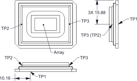 Figure 15. DMD Thermal Test Points
Micromirror array temperature can be computed analytically from measurement points on the outside of the package, the ceramic package thermal resistance, the electrical power dissipation, and the illumination heat load. The relationship between micromirror array temperature and the reference ceramic temperature is provided by the following equations:
Where:
TARRAY = Computed micromirror array temperature (°C)
TCERAMIC = Measured ceramic temperature (°C), TP1 location in Figure 15
RARRAY–TO–CERAMIC = DMD package thermal resistance from micromirror array to outside ceramic (°C/W) specified in Thermal Information
QARRAY = Total DMD power; electrical, specified in Electrical Characteristics, plus absorbed (calculated) (W)
QELECTRICAL = Nominal DMD electrical power dissipation (W), specified in Electrical Characteristics
CL2W = Conversion constant for screen lumens to absorbed optical power on the DMD (W/lm) specified below
SL = Measured ANSI screen lumens (lm)
Electrical power dissipation of the DMD is variable and depends on the voltages, data rates and operating frequencies. The nominal electrical power dissipation to use when calculating array temperature is 2.9 Watts . Absorbed optical power from the illumination source is variable and depends on the operating state of the micromirrors and the intensity of the light source. Equations shown above are valid for a 1-chip DMD system with total projection efficiency through the projection lens from DMD to the screen of 87%.
The conversion constant CL2W is based on the DMD micromirror array characteristics. It assumes a spectral efficiency of 300 lm/W for the projected light and illumination distribution of 83.7% on the DMD active array, and 16.3% on the DMD array border and window aperture. The conversion constant is calculated to be 0.00293 W/lm.
Sample Calculation for typical projection application:
TCERAMIC = 55°C, assumed system measurement; see Recommended Operating Conditions for specific limits
SL = 2000 lm
QELECTRICAL = 2.9 W (see the maximum power specifications in Electrical Characteristics)
CL2W = 0.00293 W/lm
QARRAY = 2.9 W + (0.00293 W/lm × 2000 lm) = 8.76 W
TARRAY = 55°C + (8.76 W × 0.7 × C/W) = 61.13 °C
7.7 Micromirror Landed-on/Landed-Off Duty Cycle
7.7.1 Definition of Micromirror Landed-On/Landed-Off Duty Cycle
The micromirror landed-on/landed-off duty cycle (landed duty cycle) denotes the amount of time (as a percentage) that an individual micromirror is landed in the On–state versus the amount of time the same micromirror is landed in the Off–state.
As an example, a landed duty cycle of 100/0 indicates that the referenced pixel is in the On–state 100% of the time (and in the Off–state 0% of the time); whereas 0/100 would indicate that the pixel is in the Off–state 100% of the time. Likewise, 50/50 indicates that the pixel is On 50% of the time and Off 50% of the time.
Note that when assessing landed duty cycle, the time spent switching from one state (ON or OFF) to the other state (OFF or ON) is considered negligible and is thus ignored.
Since a micromirror can only be landed in one state or the other (On or Off), the two numbers (percentages) always add to 100.
7.7.2 Landed Duty Cycle and Useful Life of the DMD
Knowing the long-term average landed duty cycle (of the end product or application) is important because subjecting all (or a portion) of the DMD’s micromirror array (also called the active array) to an asymmetric landed duty cycle for a prolonged period of time can reduce the DMD’s usable life.
Note that it is the symmetry/asymmetry of the landed duty cycle that is of relevance. The symmetry of the landed duty cycle is determined by how close the two numbers (percentages) are to being equal. For example, a landed duty cycle of 50/50 is perfectly symmetrical whereas a landed duty cycle of 100/0 or 0/100 is perfectly asymmetrical.
7.7.3 Landed Duty Cycle and Operational DMD Temperature
Operational DMD Temperature and Landed Duty Cycle interact to affect the DMD’s usable life, and this interaction can be exploited to reduce the impact that an asymmetrical Landed Duty Cycle has on the DMD’s usable life. This is quantified in the de-rating curve shown in Figure 1. The importance of this curve is that:
- All points along this curve represent the same usable life.
- All points above this curve represent lower usable life (and the further away from the curve, the lower the usable life).
- All points below this curve represent higher usable life (and the further away from the curve, the higher the usable life).
In practice, this curve specifies the Maximum Operating DMD Temperature that the DMD should be operated at for a give long-term average Landed Duty Cycle.
7.7.4 Estimating the Long-Term Average Landed Duty Cycle of a Product or Application
During a given period of time, the Landed Duty Cycle of a given pixel follows from the image content being displayed by that pixel.
For example, in the simplest case, when displaying pure-white on a given pixel for a given time period, that pixel will experience a 100/0 Landed Duty Cycle during that time period. Likewise, when displaying pure-black, the pixel will experience a 0/100 Landed Duty Cycle.
Between the two extremes (ignoring for the moment color and any image processing that may be applied to an incoming image), the Landed Duty Cycle tracks one-to-one with the gray scale value, as shown in Table 2.
Table 2. Grayscale Value and Landed Duty Cycle
| GRAYSCALE VALUE | LANDED DUTY CYCLE |
|---|---|
| 0% | 0/100 |
| 10% | 10/90 |
| 20% | 20/80 |
| 30% | 30/70 |
| 40% | 40/60 |
| 50% | 50/50 |
| 60% | 60/40 |
| 70% | 70/30 |
| 80% | 80/20 |
| 90% | 90/10 |
| 100% | 100/0 |
Accounting for color rendition (but still ignoring image processing) requires knowing both the color intensity (from 0% to 100%) for each constituent primary color (red, green, and/or blue) for the given pixel as well as the color cycle time for each primary color, where “color cycle time” is the total percentage of the frame time that a given primary must be displayed in order to achieve the desired white point.
During a given period of time, the landed duty cycle of a given pixel can be calculated as follows:
Landed Duty Cycle =(Red_Cycle_% × Red_Scale_Value) + (Green_Cycle_% × Green_Scale_Value) + (Blue_Cycle_% × Blue_Scale_Value)
Where:
Red_Cycle_%, Green_Cycle_%, and Blue_Cycle_%, represent the percentage of the frame time that Red, Green, and Blue are displayed (respectively) to achieve the desired white point.
For example, assume that the red, green and blue color cycle times are 50%, 20%, and 30% respectively (in order to achieve the desired white point), then the Landed Duty Cycle for various combinations of red, green, blue color intensities would be as shown in Table 3.
Table 3. Example Landed Duty Cycle for Full-Color
| Red Cycle Percentage 50% |
Green Cycle Percentage 20% |
Blue Cycle Percentage 30% |
Landed Duty Cycle |
|---|---|---|---|
| Red Scale Value | Green Scale Value | Blue Scale Value | |
| 0% | 0% | 0% | 0/100 |
| 100% | 0% | 0% | 50/50 |
| 0% | 100% | 0% | 20/80 |
| 0% | 0% | 100% | 30/70 |
| 12% | 0% | 0% | 6/94 |
| 0% | 35% | 0% | 7/93 |
| 0% | 0% | 60% | 18/82 |
| 100% | 100% | 0% | 70/30 |
| 0% | 100% | 100% | 50/50 |
| 100% | 0% | 100% | 80/20 |
| 12% | 35% | 0% | 13/87 |
| 0% | 35% | 60% | 25/75 |
| 12% | 0% | 60% | 24/76 |
| 100% | 100% | 100% | 100/0 |