ZHCSD21 October 2014 DLP6500FLQ
PRODUCTION DATA.
- 1 特性
- 2 应用
- 3 说明
- 4 修订历史记录
- 5 Pin Configuration and Functions
-
6 Specifications
- 6.1 Absolute Maximum Ratings
- 6.2 Handling Ratings
- 6.3 Recommended Operating Conditions
- 6.4 Thermal Information
- 6.5 Electrical Characteristics
- 6.6 Timing Requirements
- 6.7 Typical Characteristics
- 6.8 System Mounting Interface Loads
- 6.9 Micromirror Array Physical Characteristics
- 6.10 Micromirror Array Optical Characteristics
- 6.11 Window Characteristics
- 6.12 Chipset Component Usage Specification
- 7 Detailed Description
- 8 Application and Implementation
- 9 Power Supply Recommendations
- 10Layout
- 11器件和文档支持
- 12机械封装和可订购信息
5 Pin Configuration and Functions
Package Connector Terminals
(Bottom View) for FLQ (203)
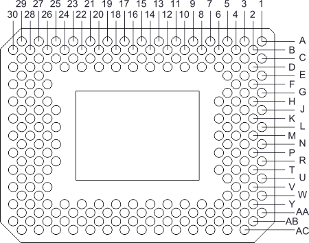
Pin Functions
| PIN(1) | TYPE (I/O/P) |
SIGNAL | DATA RATE(2) |
INTERNAL TERM(3) |
DESCRIPTION | TRACE (mils)(4) |
|
|---|---|---|---|---|---|---|---|
| NAME | NO. | ||||||
| DATA BUS A | |||||||
| D_AN(0) | B10 | Input | LVDS | DDR | Differential | Data, Negative | 557.27 |
| D_AN(1) | A13 | Input | LVDS | DDR | Differential | Data, Negative | 558.46 |
| D_AN(2) | D16 | Input | LVDS | DDR | Differential | Data, Negative | 556.87 |
| D_AN(3) | C17 | Input | LVDS | DDR | Differential | Data, Negative | 555.6 |
| D_AN(4) | B18 | Input | LVDS | DDR | Differential | Data, Negative | 555.33 |
| D_AN(5) | A17 | Input | LVDS | DDR | Differential | Data, Negative | 555.76 |
| D_AN(6) | A25 | Input | LVDS | DDR | Differential | Data, Negative | 556.47 |
| D_AN(7) | D22 | Input | LVDS | DDR | Differential | Data, Negative | 555.79 |
| D_AN(8) | C29 | Input | LVDS | DDR | Differential | Data, Negative | 556.54 |
| D_AN(9) | D28 | Input | LVDS | DDR | Differential | Data, Negative | 555.23 |
| D_AN(10) | E27 | Input | LVDS | DDR | Differential | Data, Negative | 555.55 |
| D_AN(11) | F26 | Input | LVDS | DDR | Differential | Data, Negative | 556.48 |
| D_AN(12) | G29 | Input | LVDS | DDR | Differential | Data, Negative | 555.91 |
| D_AN(13) | H28 | Input | LVDS | DDR | Differential | Data, Negative | 556.38 |
| D_AN(14) | J27 | Input | LVDS | DDR | Differential | Data, Negative | 559.01 |
| D_AN(15) | K26 | Input | LVDS | DDR | Differential | Data, Negative | 556.11 |
| D_AP(0) | B12 | Input | LVDS | DDR | Differential | Data, Positive | 555.99 |
| D_AP(1) | A11 | Input | LVDS | DDR | Differential | Data, Positive | 556.02 |
| D_AP(2) | D14 | Input | LVDS | DDR | Differential | Data, Positive | 556.31 |
| D_AP(3) | C15 | Input | LVDS | DDR | Differential | Data, Positive | 555.88 |
| D_AP(4) | B16 | Input | LVDS | DDR | Differential | Data, Positive | 556.08 |
| D_AP(5) | A19 | Input | LVDS | DDR | Differential | Data, Positive | 556.33 |
| D_AP(6) | A23 | Input | LVDS | DDR | Differential | Data, Positive | 556.13 |
| D_AP(7) | D20 | Input | LVDS | DDR | Differential | Data, Positive | 555.21 |
| D_AP(8) | A29 | Input | LVDS | DDR | Differential | Data, Positive | 555.58 |
| D_AP(9) | B28 | Input | LVDS | DDR | Differential | Data, Positive | 555.39 |
| D_AP(10) | C27 | Input | LVDS | DDR | Differential | Data, Positive | 556.11 |
| D_AP(11) | D26 | Input | LVDS | DDR | Differential | Data, Positive | 555.88 |
| D_AP(12) | F30 | Input | LVDS | DDR | Differential | Data, Positive | 556.58 |
| D_AP(13) | H30 | Input | LVDS | DDR | Differential | Data, Positive | 556.3 |
| D_AP(14) | J29 | Input | LVDS | DDR | Differential | Data, Positive | 557.67 |
| D_AP(15) | K28 | Input | LVDS | DDR | Differential | Data, Positive | 555.32 |
| DATA BUS B | |||||||
| D_BN(0) | AB10 | Input | LVDS | DDR | Differential | Data, Negative | 552.46 |
| D_BN(1) | AC13 | Input | LVDS | DDR | Differential | Data, Negative | 556.99 |
| D_BN(2) | Y16 | Input | LVDS | DDR | Differential | Data, Negative | 545.06 |
| D_BN(3) | AA17 | Input | LVDS | DDR | Differential | Data, Negative | 555.44 |
| D_BN(4) | AB18 | Input | LVDS | DDR | Differential | Data, Negative | 556.34 |
| D_BN(5) | AC17 | Input | LVDS | DDR | Differential | Data, Negative | 547.1 |
| D_BN(6) | AC25 | Input | LVDS | DDR | Differential | Data, Negative | 557.92 |
| D_BN(7) | Y22 | Input | LVDS | DDR | Differential | Data, Negative | 544.03 |
| D_BN(8) | AA29 | Input | LVDS | DDR | Differential | Data, Negative | 555.9 |
| D_BN(9) | Y28 | Input | LVDS | DDR | Differential | Data, Negative | 555.42 |
| D_BN(10) | W27 | Input | LVDS | DDR | Differential | Data, Negative | 556.26 |
| D_BN(11) | V26 | Input | LVDS | DDR | Differential | Data, Negative | 555.52 |
| D_BN(12) | T30 | Input | LVDS | DDR | Differential | Data, Negative | 556 |
| D_BN(13) | R29 | Input | LVDS | DDR | Differential | Data, Negative | 557.17 |
| D_BN(14) | R27 | Input | LVDS | DDR | Differential | Data, Negative | 555.25 |
| D_BN(15) | N27 | Input | LVDS | DDR | Differential | Data, Negative | 555.19 |
| D_BP(0) | AB12 | Input | LVDS | DDR | Differential | Data, Positive | 551.93 |
| D_BP(1) | AC11 | Input | LVDS | DDR | Differential | Data, Positive | 557.1 |
| D_BP(2) | Y14 | Input | LVDS | DDR | Differential | Data, Positive | 544.38 |
| D_BP(3) | AA15 | Input | LVDS | DDR | Differential | Data, Positive | 555.98 |
| D_BP(4) | AB16 | Input | LVDS | DDR | Differential | Data, Positive | 555.56 |
| D_BP(5) | AC19 | Input | LVDS | DDR | Differential | Data, Positive | 547.17 |
| D_BP(6) | AC23 | Input | LVDS | DDR | Differential | Data, Positive | 556.47 |
| D_BP(7) | Y20 | Input | LVDS | DDR | Differential | Data, Positive | 543.25 |
| D_BP(8) | AC29 | Input | LVDS | DDR | Differential | Data, Positive | 555.71 |
| D_BP(9) | AB28 | Input | LVDS | DDR | Differential | Data, Positive | 556.32 |
| D_BP(10) | AA27 | Input | LVDS | DDR | Differential | Data, Positive | 555.35 |
| D_BP(11) | Y26 | Input | LVDS | DDR | Differential | Data, Positive | 555.65 |
| D_BP(12) | U29 | Input | LVDS | DDR | Differential | Data, Positive | 555.28 |
| D_BP(13) | T28 | Input | LVDS | DDR | Differential | Data, Positive | 557.25 |
| D_BP(14) | P28 | Input | LVDS | DDR | Differential | Data, Positive | 555.83 |
| D_BP(15) | P26 | Input | LVDS | DDR | Differential | Data, Positive | 556.67 |
| SERIAL CONTROL | |||||||
| SCTRL_AN | C21 | Input | LVDS | DDR | Differential | Serial Control, Negative | 555.14 |
| SCTRL_BN | AA21 | Input | LVDS | DDR | Differential | Serial Control, Negative | 555.14 |
| SCTRL_AP | C23 | Input | LVDS | DDR | Differential | Serial Control, Positive | 555.13 |
| SCTRL_BP | AA23 | Input | LVDS | DDR | Differential | Serial Control, Positive | 555.13 |
| CLOCKS | |||||||
| DCLK_AN | B22 | Input | LVDS | Differential | Clock Negative | 555.12 | |
| DCLK_BN | AB22 | Input | LVDS | Differential | Clock Negative | 555.12 | |
| DCLK_AP | B24 | Input | LVDS | Differential | Clock Positive | 555.13 | |
| DCLK_BP | AB24 | Input | LVDS | Differential | Clock Positive | 555.12 | |
| SERIAL COMMUNICATIONS PORT (SCP) | |||||||
| SCP_DO | B2 | Output | LVCMOS | SDR | Serial Communications Port Output | 525.78 | |
| SCP_DI | F4 | Input | LVCMOS | SDR | Pull-Down | Serial Communications Port Data Input | 509.96 |
| SCP_CLK | E3 | Input | LVCMOS | Pull-Down | Serial Communications Port Clock | 403.93 | |
| SCP_ENZ | D4 | Input | LVCMOS | Pull-Down | Active-low Serial Communications Port Enable | 464.17 | |
| MICROMIRROR RESET CONTROL | |||||||
| RESET_ADDR(0) | C5 | Input | LVCMOS | Pull-Down | Reset Driver Address Select | 1088.3 | |
| RESET_ADDR(1) | E5 | Input | LVCMOS | Pull-Down | Reset Driver Address Select | 979.26 | |
| RESET_ADDR(2) | G5 | Input | LVCMOS | Pull-Down | Reset Driver Address Select | 900.45 | |
| RESET_ADDR(3) | AC3 | Input | LVCMOS | Pull-Down | Reset Driver Address Select | 658.56 | |
| RESET_MODE(0) | D8 | Input | LVCMOS | Pull-Down | Reset Driver Mode Select | 1012.52 | |
| RESET_MODE(1) | C11 | Input | LVCMOS | Pull-Down | Reset Driver Mode Select | 789.83 | |
| RESET_SEL(0) | T4 | Input | LVCMOS | Pull-Down | Reset Driver Level Select | 539.64 | |
| RESET_SEL(1) | U5 | Input | LVCMOS | Pull-Down | Reset Driver Level Select | 400.3 | |
| RESET_STROBE | V2 | Input | LVCMOS | Pull-Down | Reset Address, Mode, & Level latched on rising-edge | 446.34 | |
| ENABLES & INTERRUPTS | |||||||
| PWRDNZ | C3 | Input | LVCMOS | Pull-Down | Active-low Device Reset | 390.76 | |
| RESET_OEZ | W1 | Input | LVCMOS | Pull-Down | Active-low output enable for DMD reset driver circuits | 513.87 | |
| RESETZ | G3 | Input | LVCMOS | Pull-Down | Active-low sets Reset circuits in known VOFFSET state | 941.63 | |
| RESET_IRQZ | T6 | Output | LVCMOS | Active-low, output interrupt to ASIC | 403.34 | ||
| VOLTAGE REGULATOR MONITORING | |||||||
| PG_BIAS | AA11 | Input | LVCMOS | Pull-Up | Active-low fault from external VBIAS regulator | 858.86 | |
| PG_OFFSET | Y10 | Input | LVCMOS | Pull-Up | Active-low fault from external VOFFSET regulator | 822.06 | |
| PG_RESET | V4 | Input | LVCMOS | Pull-Up | Active-low fault from external VRESET regulator | 1186.98 | |
| EN_BIAS | D12 | Output | LVCMOS | Active-high enable for external VBIAS regulator | 167.53 | ||
| EN_OFFSET | AB8 | Output | LVCMOS | Active-high enable for external VOFFSET regulator | 961.04 | ||
| EN_RESET | H2 | Output | LVCMOS | Active-high enable for external VRESET regulator | 566.05 | ||
| LEAVE PIN UNCONNECTED | |||||||
| MBRST(0) | P2 | Output | Analog | Pull-Down | For proper DMD operation, do not connect | 1167.69 | |
| MBRST(1) | AB4 | Output | Analog | Pull-Down | For proper DMD operation, do not connect | 1348.04 | |
| MBRST(2) | AA7 | Output | Analog | Pull-Down | For proper DMD operation, do not connect | 1240.35 | |
| MBRST(3) | N3 | Output | Analog | Pull-Down | For proper DMD operation, do not connect | 1030.51 | |
| MBRST(4) | M4 | Output | Analog | Pull-Down | For proper DMD operation, do not connect | 870.63 | |
| MBRST(5) | AB6 | Output | Analog | Pull-Down | For proper DMD operation, do not connect | 1267.73 | |
| MBRST(6) | AA5 | Output | Analog | Pull-Down | For proper DMD operation, do not connect | 1391.22 | |
| MBRST(7) | L3 | Output | Analog | Pull-Down | For proper DMD operation, do not connect | 1064.01 | |
| MBRST(8) | Y6 | Output | Analog | Pull-Down | For proper DMD operation, do not connect | 552.89 | |
| MBRST(9) | K4 | Output | Analog | Pull-Down | For proper DMD operation, do not connect | 992.63 | |
| MBRST(10) | L5 | Output | Analog | Pull-Down | For proper DMD operation, do not connect | 1063.13 | |
| MBRST(11) | AC5 | Output | Analog | Pull-Down | For proper DMD operation, do not connect | 641.44 | |
| MBRST(12) | Y8 | Output | Analog | Pull-Down | For proper DMD operation, do not connect | 428.07 | |
| MBRST(13) | J5 | Output | Analog | Pull-Down | For proper DMD operation, do not connect | 962.91 | |
| MBRST(14) | K6 | Output | Analog | Pull-Down | For proper DMD operation, do not connect | 1093.63 | |
| MBRST(15) | AC7 | Output | Analog | Pull-Down | For proper DMD operation, do not connect | 577.13 | |
| LEAVE PIN UNCONNECTED | |||||||
| RESERVED_PFE | AA1 | Input | LVCMOS | Pull-Down | For proper DMD operation, do not connect | 1293.6 | |
| RESERVED_TM | B6 | Input | LVCMOS | Pull-Down | For proper DMD operation, do not connect | 365.64 | |
| RESERVED_XI1 | D2 | Input | LVCMOS | Pull-Down | For proper DMD operation, do not connect | 689.96 | |
| RESERVED_TP0 | Y2 | Input | Analog | For proper DMD operation, do not connect | 667.66 | ||
| RESERVED_TP1 | P6 | Input | Analog | For proper DMD operation, do not connect | 623.99 | ||
| RESERVED_TP2 | W3 | Input | Analog | For proper DMD operation, do not connect | 564.35 | ||
| LEAVE PIN UNCONNECTED | |||||||
| RESERVED_BA | U3 | Output | LVCMOS | For proper DMD operation, do not connect | 684.44 | ||
| RESERVED_BB | C9 | Output | LVCMOS | For proper DMD operation, do not connect | 223.73 | ||
| RESERVED_TS | D10 | Output | LVCMOS | For proper DMD operation, do not connect | 90.87 | ||
| LEAVE PIN UNCONNECTED | |||||||
| NO CONNECT | H6 | For proper DMD operation, do not connect | |||||
(1) The following power supplies are required to operate the DMD: VCC, VCCI, VOFFSET, VBIAS, and VRESET. VSS must also be connected.
(2) DDR = Double Data Rate.
SDR = Single Data Rate.
Refer to the Timing Requirements for specifications and relationships.
SDR = Single Data Rate.
Refer to the Timing Requirements for specifications and relationships.
(3) Internal term = CMOS level internal termination.
Refer to Recommended Operating Conditions for differential termination specification.
Refer to Recommended Operating Conditions for differential termination specification.
(4) Dielectric Constant for the DMD Type A ceramic package is approximately 9.6.
For the package trace lengths shown:
Propagation Speed = 11.8 / sqrt(9.6) = 3.808 in/ns.
Propagation Delay = 0.262 ns/in = 262 ps/in = 10.315 ps/mm.
For the package trace lengths shown:
Propagation Speed = 11.8 / sqrt(9.6) = 3.808 in/ns.
Propagation Delay = 0.262 ns/in = 262 ps/in = 10.315 ps/mm.
| PIN | TYPE (I/O/P) | SIGNAL | DESCRIPTION | |||
|---|---|---|---|---|---|---|
| NAME(1) | NO. | NO. | NO. | |||
| VBIAS | N5 | P4 | R3 | Power | Analog | Supply voltage for positive Bias level of Micromirror reset signal. |
| VBIAS | R5 | Power | Analog | Supply voltage for positive Bias level of Micromirror reset signal. | ||
| VOFFSET | G1 | J1 | L1 | Power | Analog | Supply voltage for HVCMOS logic. Supply voltage for stepped high voltage at Micromirror address electrodes. Supply voltage positive Offset level of Micromirror reset signal. |
| VOFFSET | N1 | R1 | Power | Analog | ||
| VRESET | A3 | A5 | B4 | Power | Analog | Power supply for negative reset level of mirror reset signal |
| VRESET | C7 | Power | Analog | Power supply for negative reset level of mirror reset signal | ||
| VCC | A7 | A15 | C1 | Power | Analog | Supply voltage for LVCMOS core logic. |
| VCC | E1 | U1 | AB2 | Power | Analog | Supply voltage for normal high level at Micromirror address electrodes. |
| VCC | AC9 | AC15 | Power | Analog | Supply voltage for positive Offset level of Micromirror reset signal during Power Down sequence. | |
| VCCI | A21 | A27 | D30 | Power | Analog | Power supply for LVDS Interface |
| VCCI | M30 | Y30 | AC21 | Power | Analog | Power supply for LVDS Interface |
| VCCI | AC27 | Power | Analog | Power supply for LVDS Interface | ||
| VSS | A1 | A9 | B8 | Power | Analog | Device Ground. Common return for all power. |
| VSS | B14 | B20 | B26 | Power | Analog | Device Ground. Common return for all power. |
| VSS | B30 | C13 | C19 | Power | Analog | Device Ground. Common return for all power. |
| VSS | C25 | D6 | D18 | Power | Analog | Device Ground. Common return for all power. |
| VSS | D24 | E29 | F2 | Power | Analog | Device Ground. Common return for all power. |
| VSS | F28 | G27 | H4 | Power | Analog | Device Ground. Common return for all power. |
| VSS | H26 | J3 | J25 | Power | Analog | Device Ground. Common return for all power. |
| VSS | K2 | K30 | L25 | Power | Analog | Device Ground. Common return for all power. |
| VSS | L27 | L29 | M2 | Power | Analog | Device Ground. Common return for all power. |
| VSS | M6 | M26 | M28 | Power | Analog | Device Ground. Common return for all power. |
| VSS | N25 | N29 | P30 | Power | Analog | Device Ground. Common return for all power. |
| VSS | R25 | T2 | T26 | Power | Analog | Device Ground. Common return for all power. |
| VSS | U27 | V28 | V30 | Power | Analog | Device Ground. Common return for all power. |
| VSS | W5 | W29 | Y4 | Power | Analog | Device Ground. Common return for all power. |
| VSS | Y12 | Y18 | Y24 | Power | Analog | Device Ground. Common return for all power. |
| VSS | AA3 | AA9 | AA13 | Power | Analog | Device Ground. Common return for all power. |
| VSS | AA19 | AA25 | AB14 | Power | Analog | Device Ground. Common return for all power. |
| VSS | AB20 | AB26 | AB30 | Power | Analog | Device Ground. Common return for all power. |
(1) The following power supplies are required to operate the DMD: VCC, VCCI, VOFFSET, VBIAS, and VRESET. VSS must also be connected.