SCAS640G July 2000 – August 2016 CDCVF2505
PRODUCTION DATA.
- 1 Features
- 2 Applications
- 3 Description
- 4 Revision History
- 5 Description (continued)
- 6 Pin Configuration and Functions
- 7 Specifications
- 8 Parameter Measurement Information
- 9 Detailed Description
- 10Application and Implementation
- 11Power Supply Recommendations
- 12Layout
- 13Device and Documentation Support
- 14Mechanical, Packaging, and Orderable Information
7 Specifications
7.1 Absolute Maximum Ratings
over operating free-air temperature range (unless otherwise noted)(1)| MIN | MAX | UNIT | |||
|---|---|---|---|---|---|
| VDD | Supply voltage | –0.5 | 4.3 | V | |
| VI | Input voltage(2)(3) | –0.5 | VDD + 0.5 | V | |
| VO | Output voltage(2)(3) | –0.5 | VDD + 0.5 | V | |
| IIK | Input clamp current (VI < 0 or VI > VDD) | ±50 | mA | ||
| IOK | Output clamp current (VO < 0 or VO > VDD) | ±50 | mA | ||
| IO | Continuous total output current (VO = 0 to VDD) | ±50 | mA | ||
| Tstg | Storage temperature | –65 | 150 | °C | |
(1) Stresses beyond those listed under Absolute Maximum Ratings may cause permanent damage to the device. These are stress ratings only, and functional operation of the device at these or any other conditions beyond those indicated under Recommended Operating Conditions is not implied. Exposure to absolute-maximum-rated conditions for extended periods may affect device reliability.
(2) The input and output negative-voltage ratings may be exceeded if the input and output clamp-current ratings are observed.
(3) This value is limited to 4.3 V maximum.
7.2 ESD Ratings
| VALUE | UNIT | |||
|---|---|---|---|---|
| V(ESD) | Electrostatic discharge | Human-body model (HBM), per ANSI/ESDA/JEDEC JS-001(1) | ±2000 | V |
| Charged-device model (CDM), per JEDEC specification JESD22-C101(2) | ±1000 | |||
| Machine model (MM) | ±300 | |||
(1) JEDEC document JEP155 states that 500-V HBM allows safe manufacturing with a standard ESD control process.
(2) JEDEC document JEP157 states that 250-V CDM allows safe manufacturing with a standard ESD control process.
7.3 Recommended Operating Conditions
over operating free-air temperature range (unless otherwise noted)| MIN | NOM | MAX | UNIT | ||
|---|---|---|---|---|---|
| VDD | Supply voltage | 3 | 3.3 | 3.6 | V |
| VIH | High-level input voltage | 0.7 VDD | V | ||
| VIL | Low-level input voltage | 0.3 VDD | V | ||
| VI | Input voltage | 0 | VDD | V | |
| IOH | High-level output current | –12 | mA | ||
| IOL | Low-level output current | 12 | mA | ||
| TA | Operating free-air temperature | –40 | 85 | °C | |
7.4 Thermal Information
| THERMAL METRIC(1) | CDCVF2505 | UNIT | |||
|---|---|---|---|---|---|
| D (SOIC) | PW (TSSOP) | ||||
| 8 PINS | 8 PINS | ||||
| RθJA | Junction-to-ambient thermal resistance(2) | 112.3 | 175.8 | °C/W | |
| RθJC(top) | Junction-to-case (top) thermal resistance | 55.8 | 61.8 | °C/W | |
| RθJB | Junction-to-board thermal resistance | 53.1 | 104.3 | °C/W | |
| ψJT | Junction-to-top characterization parameter | 12.8 | 7.7 | °C/W | |
| ψJB | Junction-to-board characterization parameter | 52.5 | 102.6 | °C/W | |
| RθJC(bot) | Junction-to-case (bottom) thermal resistance | — | — | °C/W | |
(1) For more information about traditional and new thermal metrics, see the Semiconductor and IC Package Thermal Metrics application report.
(2) The package thermal impedance is calculated in accordance with JESD 51.
7.5 Electrical Characteristics
over recommended operating free-air temperature range (unless otherwise noted)| PARAMETER | TEST CONDITIONS | MIN | TYP(1) | MAX | UNIT | |||
|---|---|---|---|---|---|---|---|---|
| VIK | Input voltage | II = –18 mA, VDD = 3 V | –1.2 | V | ||||
| VOH | High-level output voltage | IOH = –100 µA, VDD = MIN to MAX | VDD – 0.2 | V | ||||
| IOH = –12 mA, VDD = 3 V | 2.1 | |||||||
| IOH = –6 mA, VDD = 3 V | 2.4 | |||||||
| VOL | Low-level output voltage | IOH = 100 µA, VDD = MIN to MAX | 0.2 | V | ||||
| IOH = 12 mA, VDD = 3 V | 0.8 | |||||||
| IOH = 6 mA, VDD = 3 V | 0.55 | |||||||
| IOH | High-level output current | VO = 1 V, VDD = 3 V | –27 | mA | ||||
| VO = 1.65 V, VDD = 3.3 V | –36 | |||||||
| IOL | Low-level output current | VO = 2 V, VDD = 3 V | 27 | mA | ||||
| VO = 1.65 V, VDD = 3.3 V | 40 | |||||||
| II | Input current | VI = 0 V or VDD | ±5 | µA | ||||
| CI | Input capacitance | VI = 0 V or VDD, VDD = 3.3 V | 4.2 | pF | ||||
| Co | Output capacitance | VI = 0 V or VDD, VDD = 3.3 V | Yn | 2.8 | pF | |||
| CLKOUT | 5.2 | |||||||
(1) All typical values are at respective nominal VDD and 25°C
7.6 Timing Requirements
over recommended operating free-air temperature range (unless otherwise noted)| MIN | TYP | MAX | UNIT | |||
|---|---|---|---|---|---|---|
| SUPPLY VOLTAGE, VDD = 3.3 V ±0.3 V | ||||||
| fclk | Clock frequency | 24 | 200 | MHz | ||
| Input clock duty cycle | 24 MHz to 85 MHz(1) | 30% | 85% | |||
| 86 MHz to 200 MHz | 40% | 50% | 60% | |||
| Stabilization time(2) | 100 | µs | ||||
| SUPPLY VOLTAGE, VDD = 2.7 V | ||||||
| fclk | Clock frequency | 42 | 166 | MHz | ||
| Input clock duty cycle | 42 MHz to 85 MHz(1) | 30% | 70% | |||
| 86 MHz to 166 MHz | 40% | 50% | 60% | |||
| Stabilization time(2) | 100 | µs | ||||
(1) Assured by design but not 100% production tested
(2) Time required for the integrated PLL circuit to obtain phase lock of its feedback signal to its reference signal. For phase lock to be obtained, a fixed-frequency, fixed-phase reference signal must be present at CLKIN. Until phase lock is obtained, the specifications for propagation delay, skew, and jitter parameters given in the switching characteristics table are not applicable. This parameter does not apply for input modulation under SSC application.
7.7 Switching Characteristics
over recommended ranges of supply voltage and operating free-air temperature, CL = 25 pF, VDD = 3.3 V ±0.3 V(1)| PARAMETER | TEST CONDITIONS | MIN | TYP(2) | MAX | UNIT | |
|---|---|---|---|---|---|---|
| tpd | Propagation delay, normalized (see Figure 2) |
CLKIN to Yn, f = 66 MHz to 200 MHz | –150 | 150 | ps | |
| tsk(o) | Output skew(3) | Yn to Yn | 150 | ps | ||
| tc(jit_cc) | Jitter (cycle-to-cycle) (see Figure 4) |
f = 66 MHz to 200 MHz | 70 | 150 | ps | |
| f = 24 MHz to 50 MHz | 200 | 400 | ||||
| odc | Output duty cycle (see Figure 3) |
f = 24 MHz to 200 MHz at 50% VDD | 45% | 55% | ||
| tr | Rise time | VO = 0.4 V to 2 V | 0.5 | 2 | ns | |
| tf | Fall time | VO = 2 V to 0.4 V | 0.5 | 2 | ns | |
(1) Time required for the integrated PLL circuit to obtain phase lock of its feedback signal to its reference signal. For phase lock to be obtained, a fixed-frequency, fixed-phase reference signal must be present at CLKIN. Until phase lock is obtained, the specifications for propagation delay, skew, and jitter parameters given in the switching characteristics table are not applicable. This parameter does not apply for input modulation under SSC application.
(2) All typical values are at respective nominal VDD and 25°C
(3) The tsk(o) specification is only valid for equal loading of all outputs.
7.8 Typical Characteristics
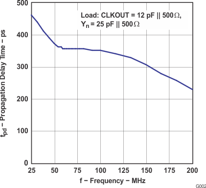
at 3.3 V, 25°C (unless otherwise noted) Figure 1. tpd, Propagation Delay Time vs Frequency
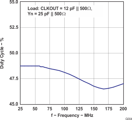
 Figure 3. Duty Cycle vs Frequency
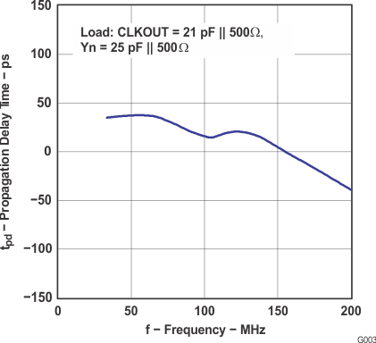
 Figure 2. tpd, Typical Propagation Delay Time
 vs Frequency (Tuned for Minimum Delay)
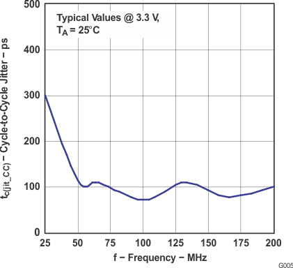
 Figure 4. Cycle-Cycle Jitter vs Frequency