SCAS640G July 2000 – August 2016 CDCVF2505
PRODUCTION DATA.
- 1 Features
- 2 Applications
- 3 Description
- 4 Revision History
- 5 Description (continued)
- 6 Pin Configuration and Functions
- 7 Specifications
- 8 Parameter Measurement Information
- 9 Detailed Description
- 10Application and Implementation
- 11Power Supply Recommendations
- 12Layout
- 13Device and Documentation Support
- 14Mechanical, Packaging, and Orderable Information
9 Detailed Description
9.1 Overview
The CDCVF2505 is designed for synchronous DRAM in server systems. This makes the device ideal for applications which require the lowest possible skew between a provided reference clock and the clock copies generated from the internal oscillator. At the same time, the phase-locked-loop has a high enough bandwidth to track a spread-spectrum reference clock.
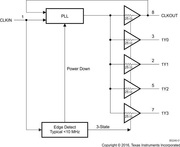
9.2 Functional Block Diagram

9.3 Feature Description
The CDCVF2505 provides a single high-impedance reference input to a phase-locked-loop circuit (PLL). The reference is directly fed to a phase comparator. The control circuit loop filter is integrated into the device. The oscillator output is fed to a clock tree with five output buffers. One of them is used as feedback to close the loop of the PLL circuit. (1) The feedback path is designed for lowest phase difference or skew seen between reference input and outputs. With respect to the supported reference frequency range the seen phase difference is negligible to the clock period. Thus the CDCVF2505 is categorized as a Zero Delay PLL.
The CDCVF2505 contains an reference clock detector. This edge detector connected to CLKIN pin automatically powers down the PLL and tri-states the output buffers to save power, as soon as the input reference frequency goes below the minimum operating frequency range.
9.4 Device Functional Modes
The device has two functional modes: active and power down.
The CDCVF2505 automatically switches from active to power down, and vice versa, when the detected CLKIN reference frequency is low. The PLL automatically switches on and tries to lock to the reference clock as soon as the input frequency exceeds 20 MHz (typical). The PLL switches off and tri-states the output buffers when the input frequency goes below 12 MHz (typical).
Table 1. Function Table
| INPUT | OUTPUTS | |
|---|---|---|
| CLKIN | 1Y (0:3) | CLKOUT |
| L | L | L |
| H | H | H |
| ≤1 MHz(1) | Z | Z |