SCAS640G July 2000 – August 2016 CDCVF2505
PRODUCTION DATA.
- 1 Features
- 2 Applications
- 3 Description
- 4 Revision History
- 5 Description (continued)
- 6 Pin Configuration and Functions
- 7 Specifications
- 8 Parameter Measurement Information
- 9 Detailed Description
- 10Application and Implementation
- 11Power Supply Recommendations
- 12Layout
- 13Device and Documentation Support
- 14Mechanical, Packaging, and Orderable Information
10 Application and Implementation
NOTE
Information in the following applications sections is not part of the TI component specification, and TI does not warrant its accuracy or completeness. TI’s customers are responsible for determining suitability of components for their purposes. Customers should validate and test their design implementation to confirm system functionality.
10.1 Application Information
The CDCVF2505 is designed for ease of use. The internal PLL operates without additional configuration required by the user.
10.2 Typical Application
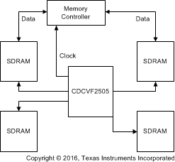
 Figure 9. Typical SDRAM Application
10.2.1 Design Requirements
The CLKOUT pin can be used to optimize the feedback delay using discrete capacitors placed at the pin to introduce additional delay on the feedback signal.
10.2.2 Detailed Design Procedure
The following steps describe how to optimize the propagation delay of the PLL:
- Determine the average output load seen by all clock outputs Y[3:0].
- Decide how the phase relationship between the CLKIN reference and the clock outputs shall be:
- zero delay
- leading CLKIN phase with respect to Y[3:0].
- lagging CLKIN phase with respect to Y[3:0].
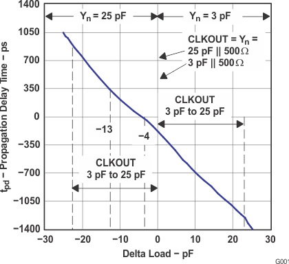
- Look up an initial typical value for the delta load using Figure 10:
- for zero delay: match the loading
- for leading CLKIN phase: load CLKOUT less than Y[3:0]
- for lagging CLKIN phase: load CLKOUT more than Y[3:0]
10.2.3 Application Curves

| Delta load = CLKOUT load – Yn load | |
| Clock frequency, f = 100 MHz |
