SCAS862G November 2008 – July 2016 CDCE62005
PRODUCTION DATA.
- 1 Features
- 2 Applications
- 3 Description
- 4 Revision History
- 5 Pin Configuration and Functions
- 6 Specifications
- 7 Parameter Measurement Information
-
8 Detailed Description
- 8.1 Overview
- 8.2 Functional Block Diagrams
- 8.3
Feature Description
- 8.3.1 Phase Noise Analysis
- 8.3.2 Output To Output Isolation
- 8.3.3 Device Control
- 8.3.4 External Control Pins
- 8.3.5
Input Block
- 8.3.5.1 Universal Input Buffers (UIB)
- 8.3.5.2 LVDS Fail Safe Mode
- 8.3.5.3 Smart Multiplexer Controls
- 8.3.5.4 Smart Multiplexer Auto Mode
- 8.3.5.5 Smart Multiplexer Dividers
- 8.3.5.6 Output Block
- 8.3.5.7 Output Multiplexer Control
- 8.3.5.8 Output Buffer Control
- 8.3.5.9 Output Buffer Control - LVCMOS Configurations
- 8.3.5.10 Output Dividers
- 8.3.5.11 Digital Phase Adjust
- 8.3.5.12 Phase Adjust Example
- 8.3.5.13 Valid Register Settings for Digital Phase Adjust Blocks
- 8.3.5.14 Output Synchronization
- 8.3.5.15 Auxiliary Output
- 8.3.5.16 Synthesizer Block
- 8.3.5.17 Input Divider
- 8.3.5.18 Feedback and Feedback Bypass Divider
- 8.3.5.19 Internal Loop Filter Component Configuration
- 8.3.5.20 External Loop Filter Component Configuration
- 8.3.6 Digital Lock Detect
- 8.3.7 Crystal Input Interference
- 8.3.8 VCO Calibration
- 8.3.9 Startup Time Estimation
- 8.3.10 Analog Lock Detect
- 8.4 Device Functional Modes
- 8.5 Programming
- 8.6
Register Maps
- 8.6.1 Device Registers: Register 0 Address 0x00
- 8.6.2 Device Registers: Register 1 Address 0x01
- 8.6.3 Device Registers: Register 2 Address 0x02
- 8.6.4 Device Registers: Register 3 Address 0x03
- 8.6.5 Device Registers: Register 4 Address 0x04
- 8.6.6 Device Registers: Register 5 Address 0x05
- 8.6.7 Device Registers: Register 6 Address 0x06
- 8.6.8 Device Registers: Register 7 Address 0x07
- 8.6.9 Device Registers: Register 8 Address 0x08
- 9 Application and Implementation
- 10Power Supply Recommendations
- 11Layout
- 12Device and Documentation Support
- 13Mechanical, Packaging, and Orderable Information
10 Power Supply Recommendations
The CDCE62005 is a high performance device. Therefore careful attention must be paid to device configuration and printed circuit board layout with respect to power consumption. Table 49 provides the power consumption for the individual blocks within the CDCE62005. To estimate total power consumption, calculate the sum of the products of the number of blocks used and the power dissipated of each corresponding block.
Table 49. CDCE62005 Power Consumption
| INTERNAL BLOCK POWER AT 3.3V (typ.) | POWER DISSIPATION/ BLOCK | NUMBER OF BLOCKS | |
|---|---|---|---|
| Input Circuit | 250 mW | 1 | |
| PLL and VCO Core | 500 mW | 1 | |
| Output Dividers | Divider = 1 | 60 mW | 5 |
| Divider > 1 | 180 mW | ||
| LVPECL Output Buffer | 75 mW(1) | 5 | |
| LVDS Output Buffer | 76 mW | 5 | |
| LVCMOS Output Buffer | Static | 7 mW | 10 |
| Transient, CL = load, fOUT = MHz output frequency, V = output swing | 3.3 × V × fOUT × (CL + 20 × 10-12) × 103 | 10 | |
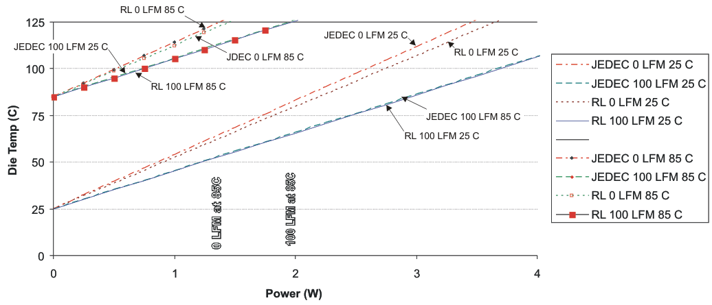
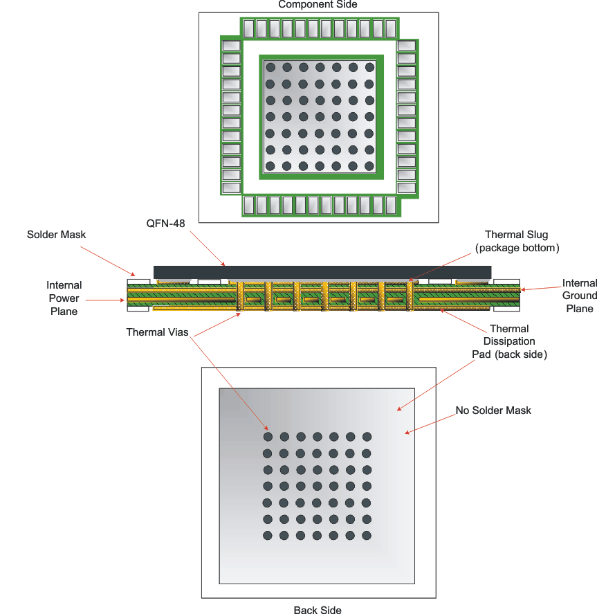
This power estimate determines the degree of thermal management required for a specific design. Employing the thermally enhanced printed circuit board layout shown in Figure 53 ensures that the thermal performance curves shown in Figure 52 apply. Observing good thermal layout practices enables the thermal pad on the backside of the QFN-48 package to provide a good thermal path between the die contained within the package and the ambient air. This thermal pad also serves as the ground connection the device. Therefore, a low inductance connection to the ground plane is essential.
Figure 53 shows a layout optimized for good thermal performance and a good power supply connection as well. The 7×7 filled via pattern facilitates both considerations. Finally, the recommended layout achieves RθJA = 27.3°C/W in still air and 20.3°C/W in an environment with 100 LFM airflow if implemented on a JEDEC compliant thermal test board..
 Figure 52. CDCE62005 Die Temperature vs Total Device Power
 Figure 53. CDCE62005 Recommended PCB Layout