SCAS862G November 2008 – July 2016 CDCE62005
PRODUCTION DATA.
- 1 Features
- 2 Applications
- 3 Description
- 4 Revision History
- 5 Pin Configuration and Functions
- 6 Specifications
- 7 Parameter Measurement Information
-
8 Detailed Description
- 8.1 Overview
- 8.2 Functional Block Diagrams
- 8.3
Feature Description
- 8.3.1 Phase Noise Analysis
- 8.3.2 Output To Output Isolation
- 8.3.3 Device Control
- 8.3.4 External Control Pins
- 8.3.5
Input Block
- 8.3.5.1 Universal Input Buffers (UIB)
- 8.3.5.2 LVDS Fail Safe Mode
- 8.3.5.3 Smart Multiplexer Controls
- 8.3.5.4 Smart Multiplexer Auto Mode
- 8.3.5.5 Smart Multiplexer Dividers
- 8.3.5.6 Output Block
- 8.3.5.7 Output Multiplexer Control
- 8.3.5.8 Output Buffer Control
- 8.3.5.9 Output Buffer Control - LVCMOS Configurations
- 8.3.5.10 Output Dividers
- 8.3.5.11 Digital Phase Adjust
- 8.3.5.12 Phase Adjust Example
- 8.3.5.13 Valid Register Settings for Digital Phase Adjust Blocks
- 8.3.5.14 Output Synchronization
- 8.3.5.15 Auxiliary Output
- 8.3.5.16 Synthesizer Block
- 8.3.5.17 Input Divider
- 8.3.5.18 Feedback and Feedback Bypass Divider
- 8.3.5.19 Internal Loop Filter Component Configuration
- 8.3.5.20 External Loop Filter Component Configuration
- 8.3.6 Digital Lock Detect
- 8.3.7 Crystal Input Interference
- 8.3.8 VCO Calibration
- 8.3.9 Startup Time Estimation
- 8.3.10 Analog Lock Detect
- 8.4 Device Functional Modes
- 8.5 Programming
- 8.6
Register Maps
- 8.6.1 Device Registers: Register 0 Address 0x00
- 8.6.2 Device Registers: Register 1 Address 0x01
- 8.6.3 Device Registers: Register 2 Address 0x02
- 8.6.4 Device Registers: Register 3 Address 0x03
- 8.6.5 Device Registers: Register 4 Address 0x04
- 8.6.6 Device Registers: Register 5 Address 0x05
- 8.6.7 Device Registers: Register 6 Address 0x06
- 8.6.8 Device Registers: Register 7 Address 0x07
- 8.6.9 Device Registers: Register 8 Address 0x08
- 9 Application and Implementation
- 10Power Supply Recommendations
- 11Layout
- 12Device and Documentation Support
- 13Mechanical, Packaging, and Orderable Information
8 Detailed Description
8.1 Overview
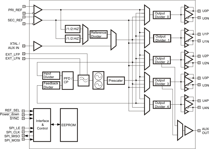
The CDCE62005 comprises of four primary blocks: the interface and control block, the input block, the output block, and the synthesizer block. In order to determine which settings are appropriate for any specific combination of input/output frequencies, a basic understanding of these blocks is required. The interface and control block determines the state of the CDCE62005 at power-up based on the contents of the on-chip EEPROM. In addition to the EEPROM, the SPI port is available to configure the CDCE62005 by writing directly to the device registers after power-up. The input block selects which of the three input ports is available for use by the synthesizer block and buffers all clock inputs. The output block provides five separate clock channels that are fully programmable and configurable to select and condition one of four internal clock sources. The synthesizer block multiplies and filters the input clock selected by the input block.
NOTE
This section provides a high-level description of the features of the CDCE62005 for purpose of understanding its capabilities. For a complete description of device registers and I/O, please refer to Device Configuration and Register Maps.
8.2 Functional Block Diagrams
8.2.1 Interface and Control Block
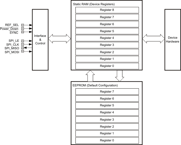
The CDCE62005 is a highly flexible and configurable architecture and as such contains a number of registers so that the user may specify device operation. The contents of nine 28-bit wide registers implemented in static RAM determine device configuration at all times. On power-up, the CDCE62005 copies the contents of the EEPROM into the RAM and the device begins operation based on the default configuration stored in the EEPROM. Systems that do not have a host system to communicate with the CDCE62005 use this method for device configuration. The CDCE62005 provides the ability to lock the EEPROM; enabling the designer to implement a fault tolerant design. After power-up, the host system may overwrite the contents of the RAM via the SPI (Serial Peripheral Interface) port. This enables the configuration and reconfiguration of the CDCE62005 during system operation. Finally, the device offers the ability to copy the contents of the RAM into EEPROM, if the EEPROM is unlocked.
8.2.2 Input Block
The Input Block includes a pair of Universal Input Buffers and an Auxiliary Input. The Input Block buffers the incoming signals and facilitates signal routing to the Internal Clock Distribution bus and the Synthesizer Block via the smart multiplexer (called the Smart MUX). The Internal Clock Distribution Bus connects to all output blocks discussed in the next section. Therefore, a clock signal present on the Internal Clock Distribution bus can appear on any or all of the device outputs. The CDCE62005 routes the PRI_REF and SEC_REF inputs directly to the Internal Clock Distribution Bus. Additionally, it can divide these signals via the dividers present on the inputs and output of the first stage of the Smart MUX.
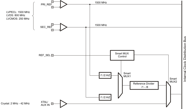 Figure 12. CDCE62005 Input Block
8.2.3 Output Block
Each of the five identical output blocks incorporates an output multiplexer, a clock divider module, and a universal output array as shown.
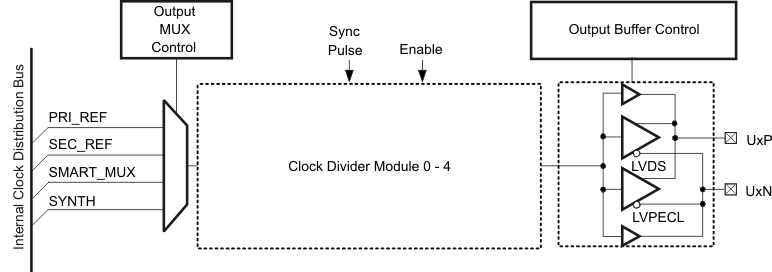 Figure 13. CDCE62005 Output Block (1 of 5)
8.2.4 Clock Divider Module 0–4
The following shows a simplified version of a Clock Divider Module (CDM). If an individual clock output channel is not used, then the user should disable the CDM and Output Buffer for the unused channel to save device power. Each channel includes two 7-bit registers to control the divide ratio used and the clock phase for each output. The output divider supports divide ratios from divide by 1 (bypass the divider) to divide by 80; the divider does not support all integer values between 1 and 80. Refer to Table 13 for a complete list of divide ratios supported.
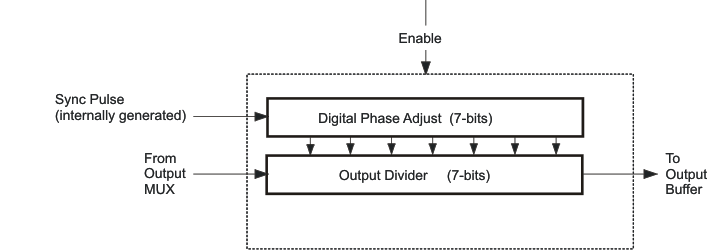 Figure 14. CDCE62005 Output Divider Module (1 of 5)
8.2.5 Synthesizer Block
Figure 15 presents a high-level overview of the Synthesizer Block on the CDCE62005.
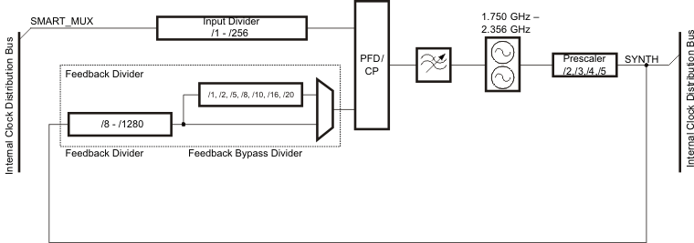 Figure 15. CDCE62005 Synthesizer Block
8.2.6 Computing The Output Frequency
Figure 16 shows the block diagram of the CDCE62005 in synthesizer mode highlighting the clock path for a single output. It also identifies the following regions containing dividers comprising the complete clock path
- R: Includes the cumulative divider values of all dividers included from the Input Ports to the output of the Smart Multiplexer (see Input Block for more details)
- O: The output divider value (see Figure 18 in Output Block for more details)
- I: The input divider value (see Synthesizer Block for more details)
- P: The prescaler divider value (see Synthesizer Block for more details)
- F: The cumulative divider value of all dividers falling within the feedback divider (see Synthesizer Block for more details)
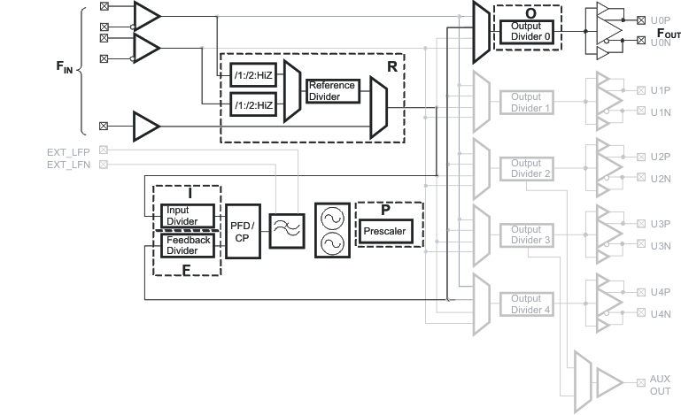 Figure 16. CDCE62005 Clock Path – Synthesizer Mode
With respect to Figure 16, any output frequency generated by the CDCE62005 relates to the input frequency connected to the Synthesizer Block by Equation 1.

Equation 1 holds true when subject to the following constraints:
The comparison frequency FCOMP is:
where:

NOTE
This device cannot output the frequencies between 785 MHz to 875 MHz
8.3 Feature Description
8.3.1 Phase Noise Analysis
Table 1. Device Output Phase Noise for 30.72 MHz External Reference(1)
| PHASE NOISE | REFERENCE 30.72 MHz |
LVPECL 491.52 MHz | LVDS 491.52 MHz | LVCMOS 122.88 MHz | UNIT | |||
|---|---|---|---|---|---|---|---|---|
| 10 Hz | –108 | –81 | –81 | –92 | dBc/Hz | |||
| 100 Hz | –130 | –94 | –96 | –108 | dBc/Hz | |||
| 1 kHz | –134 | –106 | –106 | –118 | dBc/Hz | |||
| 10 kHz | –152 | –119 | –119 | –132 | dBc/Hz | |||
| 100 kHz | –156 | –121 | –122 | –134 | dBc/Hz | |||
| 1 MHz | –157 | –131 | –131 | –143 | dBc/Hz | |||
| 10 MHz | — | –145 | –144 | –150 | dBc/Hz | |||
| 20 MHz | — | –145 | –144 | –150 | dBc/Hz | |||
| Jitter(RMS) 10k~20 MHz | 193 (10 kHz – 1 MHz) |
307 | 315 | 377 | fs | |||
PFD Frequency = 30.72 MHz, Charge Pump Current = 1.5 mA Loop BW = 400 kHz at 3.3 V and 25°C
Table 2. Device Output Phase Noise for 25 MHz Crystal Reference(1)
| PHASE NOISE | LVPECL 500 MHz | LVDS 250 MHz | LVCMOS 125 MHz | UNIT | |||
|---|---|---|---|---|---|---|---|
| 10 Hz | –57 | –62 | –68 | dBc/Hz | |||
| 100 Hz | –90 | –95 | –102 | dBc/Hz | |||
| 1 kHz | –107 | –113 | –119 | dBc/Hz | |||
| 10 kHz | –115 | –122 | –128 | dBc/Hz | |||
| 100 kHz | –118 | –124 | –130 | dBc/Hz | |||
| 1 MHz | –130 | –137 | –143 | dBc/Hz | |||
| 10 MHz | –145 | –147 | –150 | dBc/Hz | |||
| 20 MHz | –145 | –147 | –150 | dBc/Hz | |||
| Jitter(RMS) 10k~20 MHz | 389 | 405 | 437 | fs | |||
PFD Frequency = 25.00 MHz, Charge Pump Current = 1.5 mA Loop BW = 400 kHz at 3.3 V and 25°C
8.3.2 Output To Output Isolation
Table 3. Output to Output Isolation(1)
| SPUR | UNIT | |||
|---|---|---|---|---|
| Output 2 | Measured Channel | In LVPECL Signaling 15.5 MHz | –67 | db |
| Output 2 | Measured Channel | In LVPECL Signaling 93 MHz | –60 | db |
| Output 2 | Measured Channel | In LVPECL Signaling 930 MHz | –59 | db |
| Output 0 | Aggressor Channel | LVPECL 22.14 MHz | ||
| Output 1 | Aggressor Channel | LVPECL 22.14 MHz | ||
| Output 3 | Aggressor Channel | LVPECL 22.14 MHz | ||
| Output 4 | Aggressor Channel | LVPECL 22.14 MHz | ||
8.3.3 Device Control
Figure 17 provides a conceptual explanation of the CDCE62005 Device operation. Table 4 defines how the device behaves in each of the operational states.
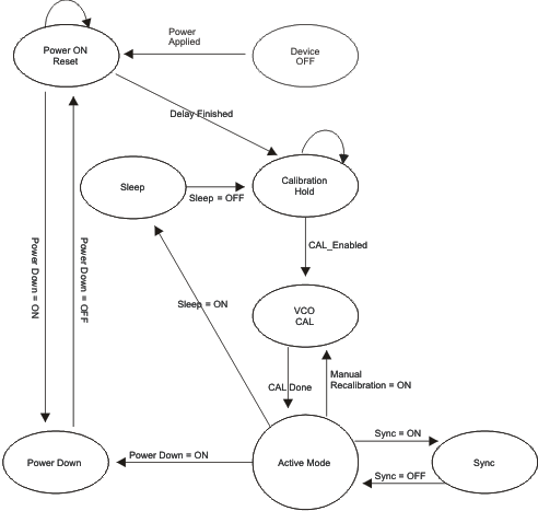 Figure 17. CDCE62005 Device State Control Diagram
Table 4. CDCE62005 Device State Definitions
8.3.4 External Control Pins
-
REF_SELREF_SEL provides a way to switch between the primary and secondary reference inputs (PRI_REF and SEC_REF) via an external signal. It works in conjunction with the smart multiplexer discussed in Input Block.
-
Power_Down The Power_Down pin places the CDCE62005 into the power down state.
The CDCE62005 loads the contents of the EEPROM into RAM after the Power_Down pin is de-asserted; therefore, it is used to initialize the device after power is applied. SPI_LE signal has to be HIGH in order for EEPROM to load correctly during the rising edge of Power_Down.
-
SYNC The SYNC pin (Active LOW) has a complementary register location located in Device Register 8 bit 8.
When enabled, Sync synchronizes all output dividers so that they begin counting simultaneously. Further, SYNC disables all outputs when in the active state.
NOTE
The output synchronization does not work for reference input frequencies less than 1 MHz.
8.3.5 Input Block
The Input Block includes two Universal Input Buffers, an Auxiliary Input, and a Smart Multiplexer. The Input Block drives three different clock signals onto the Internal Clock Distribution Bus: buffered versions of both the primary and secondary inputs (PRI_REF and SEC_REF) and the output of the Smart Multiplexer.
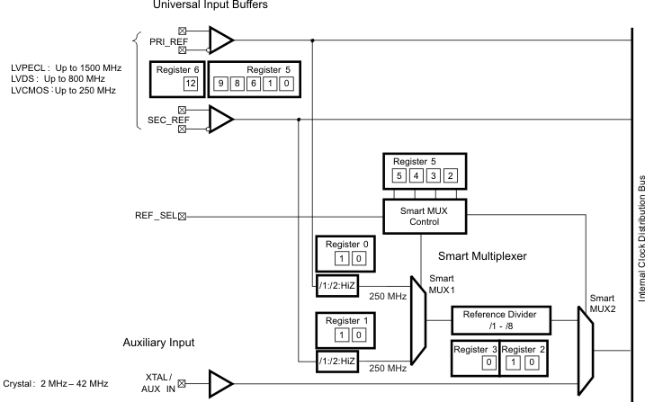 Figure 18. CDCE62005 Input Block With References to Registers
8.3.5.1 Universal Input Buffers (UIB)
Figure 19 shows the key elements of a universal input buffer. A UIB supports multiple formats along with different termination and coupling schemes. The CDCE62005 implements the UIB by including on board switched termination, a programmable bias voltage generator, and an output multiplexer. The CDCE62005 provides a high degree of configurability on the UIB to facilitate most existing clock input formats.
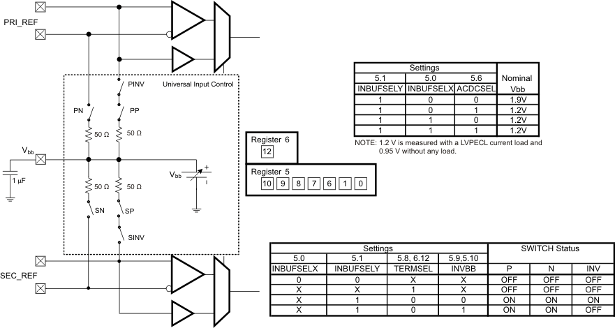 Figure 19. CDCE62005 Universal Input Buffer
Switch PP and PN will be closed only if 5.8=0 and 5.0=1 or 5.1=1.
Switch PINV will be closed only if 5.9=0 and switch SINV will be closed only if R5.10=0.
Register 5.0 and 5.6 together pick the Vbb voltage.
Table 5 lists several settings for many possible clock input scenarios. Note that the two universal input buffers share the Vbb generator. Therefore, if both inputs use internal termination, they must use the same configuration mode (LVDS, LVPECL, or LVCMOS). If the application requires different modes (for example, LVDS and LVPECL) then one of the two inputs must implement external termination.
Table 5. CDCE62005 Universal Input Buffer Configuration Matrix
| PRI_REF CONFIGURATION MATRIX | |||||||||||
|---|---|---|---|---|---|---|---|---|---|---|---|
| Register.Bit → | 5.7 | 5.1 | 5.0 | 5.8 | 5.9 | 5.6 | |||||
| Bit Name → | HYSTEN | INBUFSELY | INBUFSELX | PRI_TERMSEL | PRIINVBB | ACDCSEL | HYSTERESIS | MODE | COUPLING | TERMINATION | Vbb |
| 1 | 0 | 0 | X | X | X | ENABLED | LVCMOS | DC | N/A | — | |
| 1 | 1 | 0 | 0 | 0 | 0 | ENABLED | LVPECL | AC | Internal | 1.9V | |
| 1 | 1 | 0 | 0 | 0 | 1 | ENABLED | LVPECL | DC | Internal | 1.2V(1) | |
| 1 | 1 | 0 | 1 | X | X | ENABLED | LVPECL | — | External | — | |
| 1 | 1 | 1 | 0 | 0 | 0 | ENABLED | LVDS | AC | Internal | 1.2V | |
| 1 | 1 | 1 | 0 | 0 | 1 | ENABLED | LVDS | DC | Internal | 1.2V | |
| 1 | 1 | 1 | 1 | X | X | ENABLED | LVDS | — | External | — | |
| 0 | X | X | X | X | X | OFF | — | — | — | — | |
| 1 | X | X | X | X | X | ENABLED | — | — | — | — | |
| SEC_REF CONFIGURATION MATRIX | |||||||||||
| SETTINGS | CONFIGURATION | ||||||||||
| Register.Bit → | 5.7 | 5.1 | 5.0 | 6.12 | 5.10 | 5.6 | |||||
| Bit Name → | HYSTEN | INBUFSELY | INBUFSELX | SEC_TERMSEL | SECINVBB | ACDCSEL | Hysteresis | Mode | Coupling | Termination | Vbb |
| 1 | 0 | 0 | X | X | X | ENABLED | LVCMOS | DC | N/A | — | |
| 1 | 1 | 0 | 0 | 0 | 0 | ENABLED | LVPECL | AC | Internal | 1.9V | |
| 1 | 1 | 0 | 0 | 0 | 1 | ENABLED | LVPECL | DC | Internal | 1.2V(1) | |
| 1 | 1 | 0 | 1 | X | X | ENABLED | LVPECL | — | External | — | |
| 1 | 1 | 1 | 0 | 0 | 0 | ENABLED | LVDS | AC | Internal | 1.2V | |
| 1 | 1 | 1 | 0 | 0 | 1 | ENABLED | LVDS | DC | Internal | 1.2V | |
| 1 | 1 | 1 | 1 | X | X | ENABLED | LVDS | — | External | — | |
| 0 | X | X | X | X | X | OFF | — | — | — | — | |
| 1 | X | X | X | X | X | ENABLED | — | — | — | — | |
8.3.5.2 LVDS Fail Safe Mode
Differential receivers can switch on noise in the absence of an input signal. This occurs when the clock driver is turned off or the interconnect is damaged or missing. The traditional solution to this problem involves incorporating an external resistor network on the receiver input. This network applies a steady-state bias voltage to the input pins. The additional cost of the external components notwithstanding, the use of such a network lowers input signal magnitude and thus reduces the differential noise margin. The CDCE62005 provides internal failsafe circuitry on all LVDS inputs if enabled as shown in Table 6 for DC termination only.
Table 6. LVDS Failsafe Settings
| BIT NAME → REGISTER.BIT → |
FAILSAFE 5.11 |
LVDS FAILSAFE |
|---|---|---|
| 0 | Disabled for all inputs | |
| 1 | Enabled for all inputs |
8.3.5.3 Smart Multiplexer Controls
The smart multiplexer implements a configurable switching mechanism suitable for many applications in which fault tolerance is a design consideration. It includes the multiplexer itself along with three dividers. With respect to the multiplexer control, Table 7 provides an overview of the configurations supported by the CDCE62005.
Table 7. CDCE62005 Smart Multiplexer Settings
| REGISTER 5 SETTINGS | SMART MULTIPLEXER MODE | |||
|---|---|---|---|---|
| EECLKSEL | AUXSEL | SECSEL | PRISEL | |
| 5.5 | 5.4 | 5.3 | 5.2 | |
| 1 | 0 | 0 | 1 | Manual Mode: PRI_REF selected |
| 1 | 0 | 1 | 0 | Manual Mode: SEC_REF selected |
| 1 | 1 | 0 | 0 | Manual Mode: AUX IN selected |
| 1 | 0 | 1 | 1 | Auto Mode: PRI_REF then SEC_REF |
| 1 | 1 | 1 | 1 | Auto Mode: PRI_REF then SEC_REF then AUX IN(1) |
| 0 | 0 | 1 | 1 | REF_SEL pin selects PRI_REF or SEC_REF |
8.3.5.4 Smart Multiplexer Auto Mode
Smart Multiplexer Auto Mode switches automatically between clock inputs based on a prioritization scheme shown in Table 7. If using the Smart Multiplexer Auto Mode, the frequencies of the clock inputs may differ by up to 20%. The phase relationship between clock inputs has no restriction.
Upon the detection of a loss of signal on the highest priority clock, the smart multiplex switches its output to the next highest priority clock on the first incoming rising edge of the next highest priority clock. During this switching operation, the output of the smart multiplexer is low. Upon restoration of the higher priority clock, the smart multiplexer waits until it detects four complete cycles from the higher priority clock prior to switching the output of the smart multiplexer back to the higher priority clock. During this switching operation, the output of the smart multiplexer remains high until the next falling edge as shown in Figure 20.
 Figure 20. CDCE62005 Smart Multiplexer Timing Diagram
8.3.5.5 Smart Multiplexer Dividers
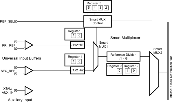 Figure 21. CDCE62005 Smart Multiplexer
The CDCE62005 Smart Multiplexer Block provides the ability to divide the primary and secondary UIB or to disconnect a UIB from the first state of the smart multiplexer altogether.
Table 8. CDCE62005 Pre-Divider Settings
| PRIMARY PRE-DIVIDER |
SECONDARY PRE-DIVIDER |
|||||||
|---|---|---|---|---|---|---|---|---|
| BIT NAME → REGISTER.BIT → |
DIV2PRIY 0.1 |
DIV2PRIX 0.0 |
DIVIDE RATIO |
BIT NAME → REGISTER.BIT → |
DIV2SECY 1.1 |
DIV2SECX 1.0 |
DIVIDE RATIO |
|
| 0 | 0 | Hi-Z | 0 | 0 | Hi-Z | |||
| 0 | 1 | /2 | 0 | 1 | /2 | |||
| 1 | 0 | /1 | 1 | 0 | /1 | |||
| 1 | 1 | Reserved | 1 | 1 | Reserved | |||
The CDCE62005 provides a Reference Divider that divides the clock exiting the first multiplexer stage; thus dividing the primary (PRI_REF) or the secondary input (SEC_REF).
Table 9. CDCE62005 Reference Divider Settings
| REFERENCE DIVIDER |
||||
|---|---|---|---|---|
| BIT NAME → REGISTER.BIT → |
REFDIV2 3.0 |
REFDIV1 2.1 |
REFDIV0 2.0 |
DIVIDE RATIO |
| 0 | 0 | 0 | /1 | |
| 0 | 0 | 1 | /2 | |
| 0 | 1 | 0 | /3 | |
| 0 | 1 | 1 | /4 | |
| 1 | 0 | 0 | /5 | |
| 1 | 0 | 1 | /6 | |
| 1 | 1 | 0 | /7 | |
| 1 | 1 | 1 | /8 | |
8.3.5.6 Output Block
The output block includes five identical output channels. Each output channel comprises an output multiplexer, a clock divider module, and a universal output buffer as shown in Figure 22.
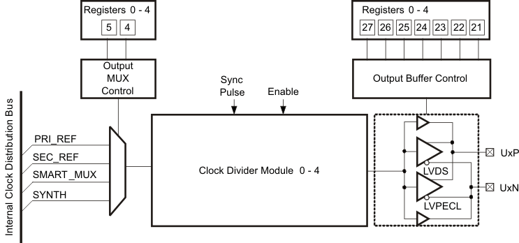 Figure 22. CDCE62005 Output Channel
8.3.5.7 Output Multiplexer Control
The Clock Divider Module receives the clock selected by the output multiplexer. The output multiplexer selects from one of four clock sources available on the Internal Clock Distribution. For a description of PRI_REF, SEC_REF, and SMART_MUX, see Figure 18. For a description of SYNTH, see Figure 28.
Table 10. CDCE62005 Output Multiplexer Control Settings
| OUTPUT MULTIPLEXER CONTROL | CLOCK SOURCE SELECTED | |
|---|---|---|
| REGISTER n (n = 0,1,2,3,4) | ||
| OUTMUXnSELX n.4 |
OUTMUXnSELY n.5 |
|
| 0 | 0 | PRI_REF |
| 0 | 1 | SEC_REF |
| 1 | 0 | SMART_MUX |
| 1 | 1 | SYNTH |
8.3.5.8 Output Buffer Control
Each of the five output channels includes a programmable output buffer; supporting LVPECL, LVDS, and LVCMOS modes. Table 11 lists the settings required to configure the CDCE62005 for each output type. Registers 0 through 4 correspond to Output Channels 0 through 4 respectively.
Table 11. CDCE62005 Output Buffer Control Settings
| OUTPUT BUFFER CONTROL | OUTPUT TYPE | |||||
|---|---|---|---|---|---|---|
| REGISTER n (n = 0,1,2,3,4) | ||||||
| CMOSMODEnPX | CMOSMODEnPY | CMOSMODEnNX | CMOSMODEnNY | OUTBUFSELnX | OUTBUFSELnY | |
| n.22 | n.23 | n.24 | n.25 | n.26 | n.27 | |
| 0 | 0 | 0 | 0 | 0 | 1 | LVPECL |
| 0 | 1 | 0 | 1 | 1 | 1 | LVDS |
| See LVCMOS Output Buffer Configuration Settings | 0 | 0 | LVCMOS | |||
| 0 | 1 | 0 | 1 | 1 | 0 | Disabled to High-Z |
8.3.5.9 Output Buffer Control – LVCMOS Configurations
A LVCMOS output configuration requires additional configuration data. In the single ended configuration, each Output Channel provides a pair of outputs. The CDCE62005 supports four modes of operation for single ended outputs as listed in Table 12.
Table 12. LVCMOS Output Buffer Configuration Settings
| OUTPUT BUFFER CONTROL – LVCMOS CONFIGURATION | OUTPUT TYPE |
PIN | OUTPUT MODE | |||||
|---|---|---|---|---|---|---|---|---|
| REGISTER n (n = 0,1,2,3,4) | ||||||||
| CMOSMODEnPX | CMOSMODEnPY | CMOSMODEnNX | CMOSMODEnNY | OUTBUFSELnX | OUTBUFSELnY | |||
| n.22 | n.23 | n.24 | n.25 | n.26 | n.27 | |||
| X | X | 0 | 0 | 0 | 0 | LVCMOS | Negative | Active – Non-inverted |
| X | X | 0 | 1 | 0 | 0 | LVCMOS | Negative | Hi-Z |
| X | X | 1 | 0 | 0 | 0 | LVCMOS | Negative | Active – Non-inverted |
| X | X | 1 | 1 | 0 | 0 | LVCMOS | Negative | Low |
| 0 | 0 | X | X | 0 | 0 | LVCMOS | Positive | Active – Non-inverted |
| 0 | 1 | X | X | 0 | 0 | LVCMOS | Positive | Hi-Z |
| 1 | 0 | X | X | 0 | 0 | LVCMOS | Positive | Active – Non-inverted |
| 1 | 1 | X | X | 0 | 0 | LVCMOS | Positive | Low |
8.3.5.10 Output Dividers
Figure 23 shows that each output channel provides a 7-bit divider and digital phase adjust block. The Table 13 lists the divide ratios supported by the output divider for each output channel. Figure 24 illustrates the output divider architecture in detail. The Prescaler provides an array of low noise dividers with duty cycle correction. The Integer Divider includes a final divide by two stage which is used to correct the duty cycle of the /1–/8 stage. The output divider’s maximum input frequency is limited to 1.175 GHz. If the divider is bypassed (divide ratio = 1) then the maximum frequency of the output channel is 1.5 GHz.
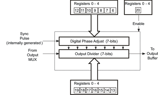 Figure 23. CDCE62005 Output Divider and Phase Adjust
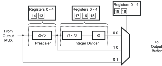 Figure 24. CDCE62005 Output Divider Architecture
Table 13. CDCE62005 Output Divider Settings(1)
| OUTPUT DIVIDER n SETTINGS REGISTER (n = 0,1,2,3,4) | OUTPUT DIVIDE RATIO |
||||||||||
|---|---|---|---|---|---|---|---|---|---|---|---|
| MULTIPLEXER | INTEGER DIVIDER | PRESCALER | |||||||||
| OUTn- DIVSEL6 |
OUTn- DIVSEL5 |
OUTn- DIVSEL4 |
OUTn- DIVSEL3 |
OUTn- DIVSEL2 |
OUTn- DIVSEL1 |
OUTn- DIVSEL0 |
OUTn- DIVSEL |
PRESCALER SETTING |
INTEGER DIVIDER SETTING |
||
| n.19 | n.18 | n.17 | n.16 | n.15 | n.14 | n.13 | n.20 | OUTPUT |
|||
| CHANNELS |
AUXILIARY |
||||||||||
| 0-4 | OUTPUT | ||||||||||
| X | X | X | X | X | X | X | 0 | OFF | OFF | ||
| 0 | 1 | 0 | 0 | 0 | 0 | 0 | 1 | – | – | 1 | OFF |
| 1 | 0 | 0 | 0 | 0 | 0 | 0 | 1 | 2 | – | 2* | 4 |
| 1 | 0 | 0 | 0 | 0 | 0 | 1 | 1 | 3 | – | 3* | 6 |
| 1 | 0 | 0 | 0 | 0 | 1 | 0 | 1 | 4 | – | 4 | 8 |
| 1 | 0 | 0 | 0 | 0 | 1 | 1 | 1 | 5 | – | 5 | 10 |
| 0 | 0 | 0 | 0 | 0 | 0 | 1 | 1 | 3 | 2 | 6 | 6 |
| 0 | 0 | 0 | 0 | 0 | 1 | 0 | 1 | 4 | 2 | 8 | 8 |
| 0 | 0 | 0 | 0 | 0 | 1 | 1 | 1 | 5 | 2 | 10 | 10 |
| 0 | 0 | 0 | 0 | 1 | 0 | 1 | 1 | 3 | 4 | 12 | 12 |
| 0 | 0 | 0 | 0 | 1 | 1 | 0 | 1 | 4 | 4 | 16 | 16 |
| 0 | 0 | 0 | 0 | 1 | 1 | 1 | 1 | 5 | 4 | 20 | 20 |
| 0 | 0 | 0 | 1 | 0 | 0 | 1 | 1 | 3 | 6 | 18 | 18 |
| 0 | 0 | 0 | 1 | 0 | 1 | 0 | 1 | 4 | 6 | 24 | 24 |
| 0 | 0 | 0 | 1 | 0 | 1 | 1 | 1 | 5 | 6 | 30 | 30 |
| 0 | 0 | 0 | 1 | 1 | 1 | 0 | 1 | 4 | 8 | 32 | 32 |
| 0 | 0 | 0 | 1 | 1 | 1 | 1 | 1 | 5 | 8 | 40 | 40 |
| 0 | 0 | 1 | 0 | 0 | 1 | 1 | 1 | 5 | 10 | 50 | 50 |
| 0 | 0 | 1 | 0 | 1 | 0 | 1 | 1 | 3 | 12 | 36 | 36 |
| 0 | 0 | 1 | 0 | 1 | 1 | 0 | 1 | 4 | 12 | 48 | 48 |
| 0 | 0 | 1 | 0 | 1 | 1 | 1 | 1 | 5 | 12 | 60 | 60 |
| 0 | 0 | 1 | 1 | 0 | 0 | 0 | 1 | 2 | 14 | 28 | 28 |
| 0 | 0 | 1 | 1 | 0 | 0 | 1 | 1 | 3 | 14 | 42 | 42 |
| 0 | 0 | 1 | 1 | 0 | 1 | 0 | 1 | 4 | 14 | 56 | 56 |
| 0 | 0 | 1 | 1 | 0 | 1 | 1 | 1 | 5 | 14 | 70 | 70 |
| 0 | 0 | 1 | 1 | 1 | 1 | 0 | 1 | 4 | 16 | 64 | 64 |
| 0 | 0 | 1 | 1 | 1 | 1 | 1 | 1 | 5 | 16 | 80 | 80 |
8.3.5.11 Digital Phase Adjust
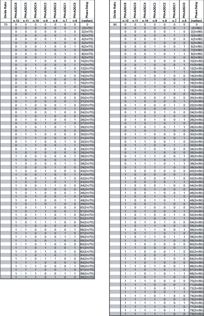
Figure 25 provides an overview of the Digital Phase Adjust feature. The output divider includes a coarse phase adjust that shifts the divided clock signal that drives the output buffer. Essentially, the Digital Phase Adjust timer delays when the output divider starts dividing; thereby shifting the phase of the output clock. The phase adjust resolution is a function of the divide function. Coarse phase adjust parameters include:
-
Number of phase delay steps the number of phase delay steps available is equal to the divide ratio selected.
For example, if a Divide by 4 is selected, then the Digital Phase Adjust can be programmed to select when the output divider changes state based upon selecting one of the four counts on the input. Figure 25 shows an example of divide by 16 in which there are 16 rising edges of Clock IN at which the output divider changes state (this particular example shows the fourth edge shifting the output by one fourth of the period of the output).
-
Phase delay step size the step size is determined by the number of phase delay steps according to the following equations:


 Figure 25. CDCE62005 Phase Adjust
8.3.5.12 Phase Adjust Example
Given:
- Output Frequency = 30.72 MHz
- VCO Operating Frequency = 1966.08 MHz
- Prescaler Divider Setting = 4
- Output Divider Setting = 16

8.3.5.13 Valid Register Settings for Digital Phase Adjust Blocks
Table 14 through Table 19 provide a list of valid register settings for the digital phase adjust blocks.
Table 14. CDCE62005 Output Coarse Phase Adjust Settings (1)
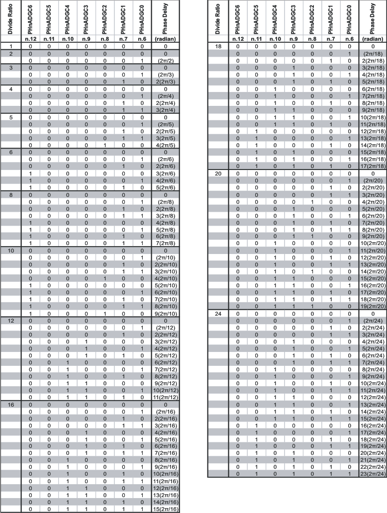 |
Table 15. CDCE62005 Output Coarse Phase Adjust Settings (2)
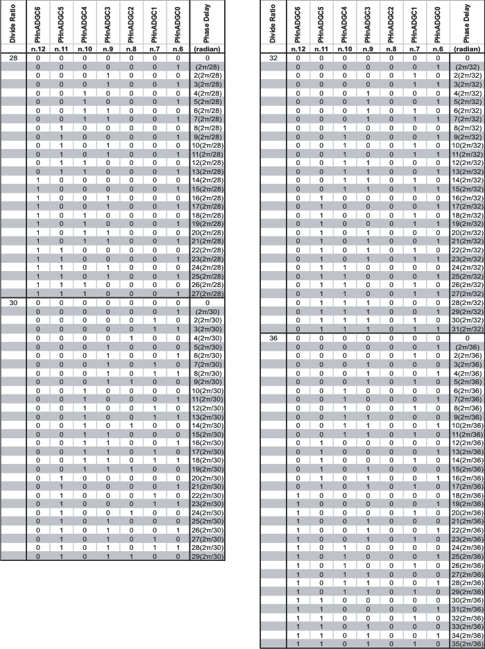 |
Table 16. CDCE62005 Output Coarse Phase Adjust Settings (3)
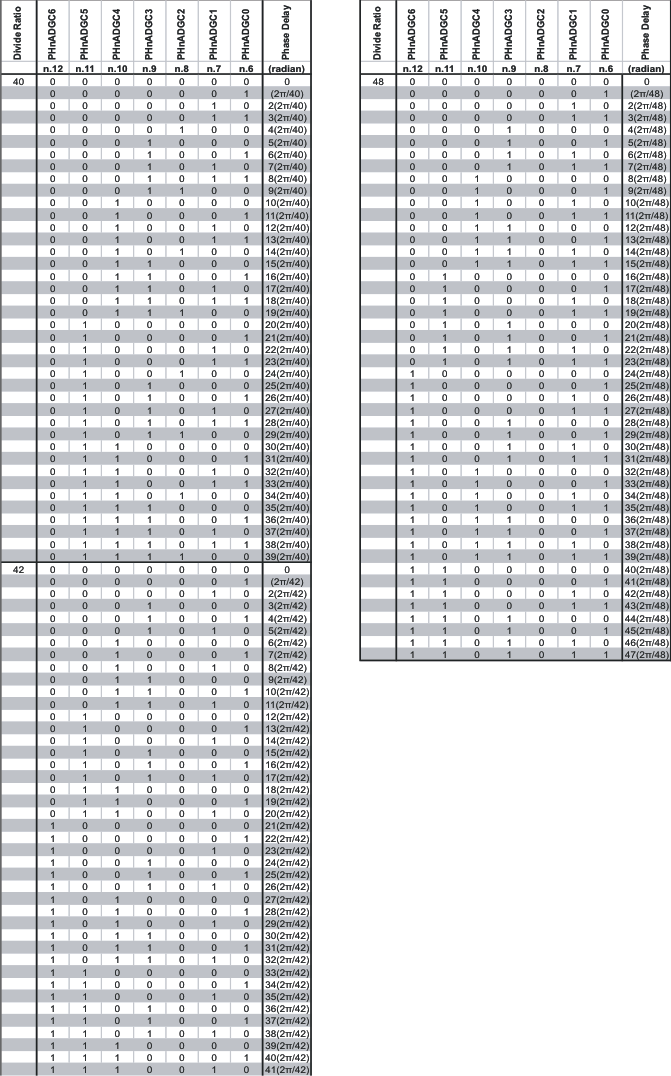 |
Table 17. CDCE62005 Output Coarse Phase Adjust Settings (4)
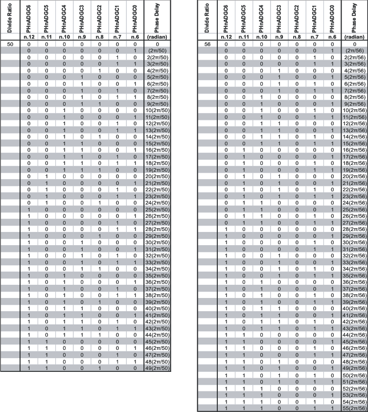 |
Table 18. CDCE62005 Output Coarse Phase Adjust Settings (5)
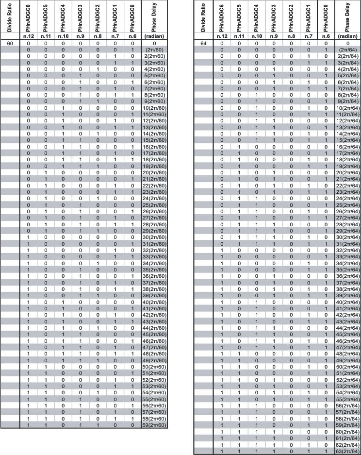 |
Table 19. CDCE62005 Output Coarse Phase Adjust Settings (6)
 |
8.3.5.14 Output Synchronization
Figure 26 shows the output synchronization circuitry and relative output clock phase position with respect to SYNC signal Low to High phase transition.
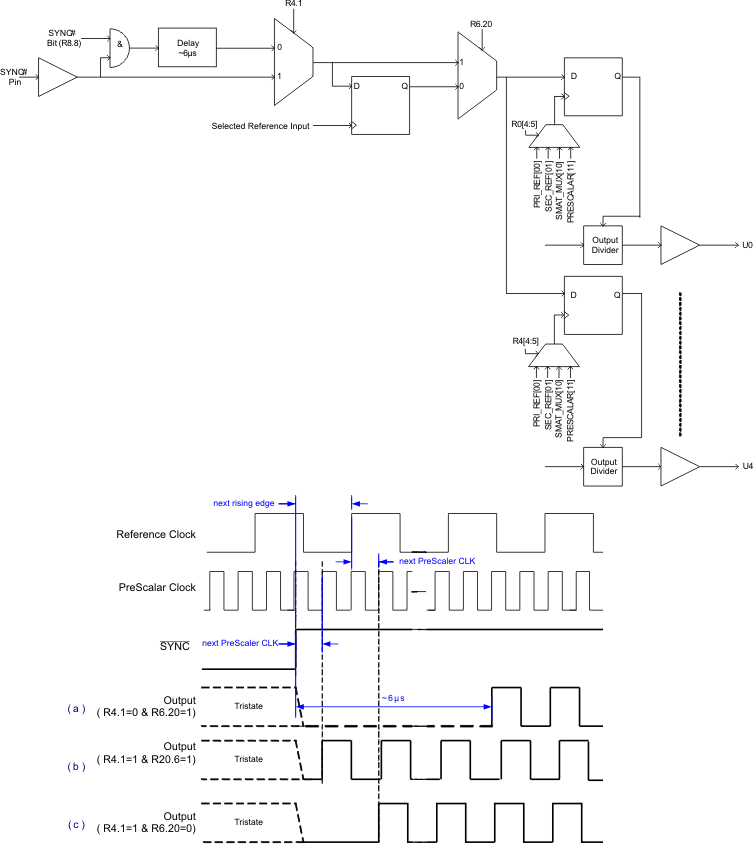
NOTE:
The signal diagram is based on the assumption that prescalar clock is selected by output Mux ( Rn[4:5] where n = 0, 1, 2, 3 or 4)The synchronization of the outputs can be accomplished by toggling the SYNC pin, or Bit (R8.8), or by changing any output divider values. Table 20 shows the phase relationship between output phase and the SYNC signal, the selected reference clock and the prescalar output clock phases.
Table 20. Output Synchronization Procedure
| R4.1 | R6.20 | COMMENTS | |
|---|---|---|---|
| Toggling SYNC Pin or Bit (R8.8) from low to high | 0 | 0 | The synchronized outputs will be enabled after ~6 µs delay and the next rising edge of the reference clock and selected clock of output multiplexer. |
| 0 | 1 | The synchronized outputs will be enabled after ~6 µs delay and the next rising edge of selected clock of output multiplexer (reference Figure 26 (a)). | |
| 1 | 0 | The synchronized outputs will be enabled with the next rising edge of reference clock & the selected clock of output multiplexer (reference Figure 26 (c)). | |
| 1 | 1 | The synchronized outputs will be enabled with the next rising edge of the selected clock of output multiplexer (reference Figure 26 (b)). | |
| Toggling SYNC Pin or Bit (R8.8) from high to low | X | X | All outputs are disabled. |
8.3.5.15 Auxiliary Output
Figure 27 shows the auxiliary output port. Table 21 lists how the auxiliary output port is controlled. The output buffer supports a maximum output frequency of 250 MHz and drives at LVCMOS levels. Refer to Table 13 for the list of divider settings that establishes the output frequency.
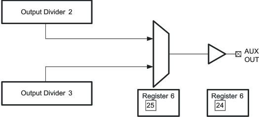 Figure 27. CDCE62005 Auxiliary Output
Table 21. CDCE62005 Auxiliary Output Settings
| BIT NAME → | AUXFEEDSEL | AUXOUTEN | AUX OUTPUT SOURCE |
|---|---|---|---|
| REGISTER.BIT → | 6.25 | 6.24 | |
| X | 0 | OFF | |
| 0 | 1 | Divider 2(1) | |
| 1 | 1 | Divider 3(1) |
8.3.5.16 Synthesizer Block
Figure 28 provides an overview of the CDCE62005 synthesizer block. The Synthesizer Block provides a Phase Locked Loop, a partially integrated programmable loop filter, and two Voltage Controlled Oscillators (VCO). The synthesizer block generates an output clock called “SYNTH” and drives it onto the Internal Clock Distribution Bus.
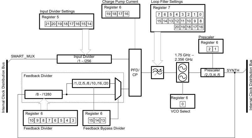 Figure 28. CDCE62005 Synthesizer Block
8.3.5.17 Input Divider
The Input Divider divides the clock signal selected by the Smart Multiplexer (see Table 7) and presents the divided signal to the Phase Frequency Detector / Charge Pump of the frequency synthesizer.
Table 22. CDCE62005 Input Divider Settings
| INPUT DIVIDER SETTINGS | DIVIDE RATIO | |||||||
|---|---|---|---|---|---|---|---|---|
| SELINDIV7 | SELINDIV6 | SELINDIV5 | SELINDIV4 | SELINDIV3 | SELINDIV2 | SELINDIV1 | SELINDIV0 | |
| 5.21 | 5.20 | 5.19 | 5.18 | 5.17 | 5.16 | 5.15 | 5.14 | |
| 0 | 0 | 0 | 0 | 0 | 0 | 0 | 0 | 1 |
| 0 | 0 | 0 | 0 | 0 | 0 | 0 | 1 | 2 |
| 0 | 0 | 0 | 0 | 0 | 0 | 1 | 0 | 3 |
| 0 | 0 | 0 | 0 | 0 | 0 | 1 | 1 | 4 |
| 0 | 0 | 0 | 0 | 0 | 1 | 0 | 0 | 5 |
| 0 | 0 | 0 | 0 | 0 | 1 | 0 | 1 | 6 |
| • | • | • | • | • | • | • | • | • |
| • | • | • | • | • | • | • | • | • |
| 1 | 1 | 1 | 1 | 1 | 1 | 1 | 1 | 256 |
8.3.5.18 Feedback and Feedback Bypass Divider
Table 23 shows how to configure the Feedback divider for various divide values
Table 23. CDCE62005 Feedback Divider Settings
| FEEDBACK DIVIDER | DIVIDE RATIO | |||||||
|---|---|---|---|---|---|---|---|---|
| SELFBDIV7 | SELFBDIV6 | SELFBDIV5 | SELFBDIV4 | SELFBDIV3 | SELFBDIV2 | SELFBDIV1 | SELFBDIV0 | |
| 6.10 | 6.9 | 9.8 | 6.7 | 6.6 | 6.5 | 6.4 | 6.3 | |
| 0 | 0 | 0 | 0 | 0 | 0 | 0 | 0 | 8 |
| 0 | 0 | 0 | 0 | 0 | 0 | 0 | 1 | 12 |
| 0 | 0 | 0 | 0 | 0 | 0 | 1 | 0 | 16 |
| 0 | 0 | 0 | 0 | 0 | 0 | 1 | 1 | 20 |
| 0 | 0 | 0 | 0 | 0 | 1 | 0 | 1 | 24 |
| 0 | 0 | 0 | 0 | 0 | 1 | 1 | 0 | 32 |
| 0 | 0 | 0 | 0 | 1 | 0 | 0 | 1 | 36 |
| 0 | 0 | 0 | 0 | 0 | 1 | 1 | 1 | 40 |
| 0 | 0 | 0 | 0 | 1 | 0 | 1 | 0 | 48 |
| 0 | 0 | 0 | 1 | 1 | 0 | 0 | 0 | 56 |
| 0 | 0 | 0 | 0 | 1 | 0 | 1 | 1 | 60 |
| 0 | 0 | 0 | 0 | 1 | 1 | 1 | 0 | 64 |
| 0 | 0 | 0 | 1 | 0 | 1 | 0 | 1 | 72 |
| 0 | 0 | 0 | 0 | 1 | 1 | 1 | 1 | 80 |
| 0 | 0 | 0 | 1 | 1 | 0 | 0 | 1 | 84 |
| 0 | 0 | 0 | 1 | 0 | 1 | 1 | 0 | 96 |
| 0 | 0 | 0 | 1 | 0 | 0 | 1 | 1 | 100 |
| 0 | 1 | 0 | 0 | 1 | 0 | 0 | 1 | 108 |
| 0 | 0 | 0 | 1 | 1 | 0 | 1 | 0 | 112 |
| 0 | 0 | 0 | 1 | 0 | 1 | 1 | 1 | 120 |
| 0 | 0 | 0 | 1 | 1 | 1 | 1 | 0 | 128 |
| 0 | 0 | 0 | 1 | 1 | 0 | 1 | 1 | 140 |
| 0 | 0 | 1 | 1 | 0 | 1 | 0 | 1 | 144 |
| 0 | 0 | 0 | 1 | 1 | 1 | 1 | 1 | 160 |
| 0 | 0 | 1 | 1 | 1 | 0 | 0 | 1 | 168 |
| 0 | 1 | 0 | 0 | 1 | 0 | 1 | 1 | 180 |
| 0 | 0 | 1 | 1 | 0 | 1 | 1 | 0 | 192 |
| 0 | 0 | 1 | 1 | 0 | 0 | 1 | 1 | 200 |
| 0 | 1 | 0 | 1 | 0 | 1 | 0 | 1 | 216 |
| 0 | 0 | 1 | 1 | 1 | 0 | 1 | 0 | 224 |
| 0 | 0 | 1 | 1 | 0 | 1 | 1 | 1 | 240 |
| 0 | 1 | 0 | 1 | 1 | 0 | 0 | 1 | 252 |
| 0 | 0 | 1 | 1 | 1 | 1 | 1 | 0 | 256 |
| 0 | 0 | 1 | 1 | 1 | 0 | 1 | 1 | 280 |
| 0 | 1 | 0 | 1 | 0 | 1 | 1 | 0 | 288 |
| 0 | 1 | 0 | 1 | 0 | 0 | 1 | 1 | 300 |
| 0 | 0 | 1 | 1 | 1 | 1 | 1 | 1 | 320 |
| 0 | 1 | 0 | 1 | 1 | 0 | 1 | 0 | 336 |
| 0 | 1 | 0 | 1 | 0 | 1 | 1 | 1 | 360 |
| 0 | 1 | 0 | 1 | 1 | 1 | 1 | 0 | 384 |
| 1 | 1 | 0 | 1 | 1 | 0 | 0 | 0 | 392 |
| 0 | 1 | 1 | 1 | 0 | 0 | 1 | 1 | 400 |
| 0 | 1 | 0 | 1 | 1 | 0 | 1 | 1 | 420 |
| 1 | 0 | 1 | 1 | 0 | 1 | 0 | 1 | 432 |
| 0 | 1 | 1 | 1 | 1 | 0 | 1 | 0 | 448 |
| 0 | 1 | 0 | 1 | 1 | 1 | 1 | 1 | 480 |
| 1 | 0 | 0 | 1 | 0 | 0 | 1 | 1 | 500 |
| 1 | 0 | 1 | 1 | 1 | 0 | 0 | 1 | 504 |
| 0 | 1 | 1 | 1 | 1 | 1 | 1 | 0 | 512 |
| 0 | 1 | 1 | 1 | 1 | 0 | 1 | 1 | 560 |
| 1 | 0 | 1 | 1 | 0 | 1 | 1 | 0 | 576 |
| 1 | 1 | 0 | 1 | 1 | 0 | 0 | 1 | 588 |
| 1 | 0 | 0 | 1 | 0 | 1 | 1 | 1 | 600 |
| 0 | 1 | 1 | 1 | 1 | 1 | 1 | 1 | 640 |
| 1 | 0 | 1 | 1 | 1 | 0 | 1 | 0 | 672 |
| 1 | 0 | 0 | 1 | 1 | 0 | 1 | 1 | 700 |
| 1 | 0 | 1 | 1 | 0 | 1 | 1 | 1 | 720 |
| 1 | 0 | 1 | 1 | 1 | 1 | 1 | 0 | 768 |
| 1 | 1 | 0 | 1 | 1 | 0 | 1 | 0 | 784 |
| 1 | 0 | 0 | 1 | 1 | 1 | 1 | 1 | 800 |
| 1 | 0 | 1 | 1 | 1 | 0 | 1 | 1 | 840 |
| 1 | 1 | 0 | 1 | 1 | 1 | 1 | 0 | 896 |
| 1 | 0 | 1 | 1 | 1 | 1 | 1 | 1 | 960 |
| 1 | 1 | 0 | 1 | 1 | 0 | 1 | 1 | 980 |
| 1 | 1 | 1 | 1 | 1 | 1 | 1 | 0 | 1024 |
| 1 | 1 | 0 | 1 | 1 | 1 | 1 | 1 | 1120 |
| 1 | 1 | 1 | 1 | 1 | 1 | 1 | 1 | 1280 |
Table 24 shows how to configure the Feedback Bypass Divider.
Table 24. CDCE62005 Feedback Bypass Divider Settings
| FEEDBACK BYPASS DIVIDER | DIVIDE RATIO | ||
|---|---|---|---|
| SELBPDIV2 | SELBPDIV1 | SELBPDIV0 | |
| 6.15 | 6.14 | 6.13 | |
| 0 | 0 | 0 | 2 |
| 0 | 0 | 1 | 5 |
| 0 | 1 | 0 | 8 |
| 0 | 1 | 1 | 10 |
| 1 | 0 | 0 | 16 |
| 1 | 0 | 1 | 20 |
| 1 | 1 | 0 | RESERVED |
| 1 | 1 | 1 | 1(bypass) |
8.3.5.18.1 VCO Select
Table 25 illustrates how to control the dual voltage controlled oscillators.
Table 25. CDCE62005 VCO Select
| BIT NAME → REGISTER.BIT → |
VCO SELECT SELVCO |
VCO CHARACTERISTICS | ||
|---|---|---|---|---|
| 6.0 | VCO RANGE | Fmin (MHz) | Fmax (MHz) | |
| 0 | Low | 1750 | 2046 | |
| 1 | High | 2040 | 2356 | |
8.3.5.18.2 Prescaler
Table 26 shows how to configure the prescaler.
Table 26. CDCE62005 Prescaler Settings
| SETTINGS | DIVIDE RATIO | |
|---|---|---|
| SELPRESCB | SELPRESCA | |
| 6.2 | 6.1 | |
| 0 | 0 | 5 |
| 1 | 0 | 4 |
| 0 | 1 | 3 |
| 1 | 1 | 2 |
8.3.5.18.3 Charge Pump Current Settings
Table 27 provides the settings for the charge pump:
Table 27. CDCD62005 Charge Pump Settings
| BIT NAME → REGISTER.BIT → |
CHARGE PUMP SETTINGS | CHARGE PUMP CURRENT | |||
|---|---|---|---|---|---|
| ICPSEL3 | ICPSEL2 | ICPSEL1 | ICPSEL0 | ||
| 6.19 | 6.18 | 6.17 | 6.16 | ||
| 0 | 0 | 0 | 0 | 50 μA | |
| 0 | 0 | 0 | 1 | 100 μA | |
| 0 | 0 | 1 | 0 | 150 μA | |
| 0 | 0 | 1 | 1 | 200 μA | |
| 0 | 1 | 0 | 0 | 300 μA | |
| 0 | 1 | 0 | 1 | 400 μA | |
| 0 | 1 | 1 | 0 | 600 μA | |
| 0 | 1 | 1 | 1 | 750 μA | |
| 1 | 0 | 0 | 0 | 1 mA | |
| 1 | 0 | 0 | 1 | 1.25 mA | |
| 1 | 0 | 1 | 0 | 1.5 mA | |
| 1 | 0 | 1 | 1 | 2 mA | |
| 1 | 1 | 0 | 0 | 2.5 mA | |
| 1 | 1 | 0 | 1 | 3 mA | |
| 1 | 1 | 1 | 0 | 3.5 mA | |
| 1 | 1 | 1 | 1 | 3.75 mA | |
8.3.5.18.4 Loop Filter
Figure 29 depicts the loop filter topology of the CDCE62005. It facilitates both internal and external implementations providing optimal flexibility.
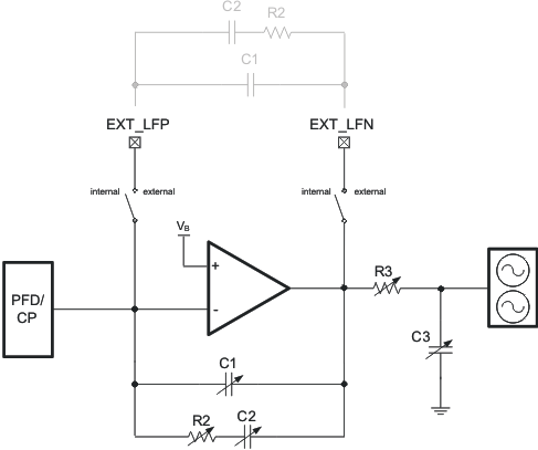 Figure 29. CDCE62005 Loop Filter Topology
8.3.5.19 Internal Loop Filter Component Configuration
Figure 29 contains five different loop filter components with programmable values: C1, C2, R2, R3, and C3. Table 28 shows that the CDCE62005 uses one of four different types of circuit implementation (shown in Figure 30) for each of the internal loop filter components.
Table 28. CDCE62005 Loop Filter Component Implementation Type
| COMPONENT | CONTROL BITS USED | IMPLEMENTATION TYPE (see Figure 30) |
|---|---|---|
| C1 | 5 | a |
| C2 | 5 | a |
| R2 | 5 | c |
| R3 | 2 | d |
| C3 | 4 | b |
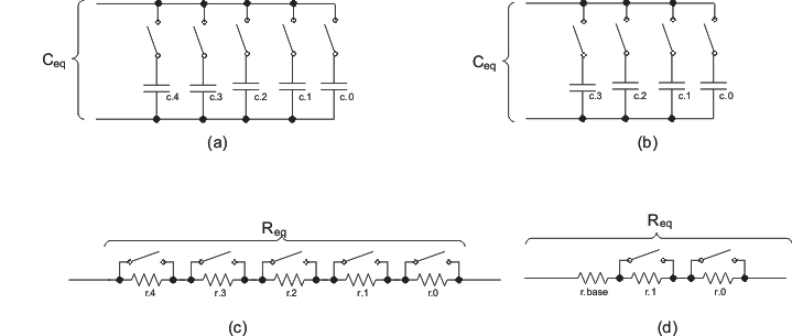 Figure 30. CDCE62005 Internal Loop Filter Component Schematics
Table 29. CDCE62005 Internal Loop Filter – C1 Settings
| C1 SETTINGS | CAPACITOR VALUE | ||||||
|---|---|---|---|---|---|---|---|
| BIT NAME → | EXLFSEL | LFRCSEL14 | LFRCSEL13 | LFRCSEL12 | LFRCSEL11 | LFRCSEL10 | |
| CAPACITOR VALUE → | — | 37.5 pF | 21.5 pF | 10 pF | 6.5 pF | 1.5 pF | |
| REGISTER.BIT → | 6.26 | 7.14 | 7.13 | 7.12 | 7.11 | 7.10 | |
| 1 | 0 | 0 | 0 | 0 | 0 | External Loop Filter | |
| 0 | 0 | 0 | 0 | 0 | 0 | 0 pF | |
| 0 | 0 | 0 | 0 | 0 | 1 | 1.5 pF | |
| 0 | 0 | 0 | 0 | 1 | 0 | 6.5 pF | |
| 0 | 0 | 0 | 0 | 1 | 1 | 8 pF | |
| 0 | 0 | 0 | 1 | 0 | 0 | 10 pF | |
| 0 | 0 | 0 | 1 | 0 | 1 | 11.5 pF | |
| 0 | 0 | 0 | 1 | 1 | 0 | 16.5 pF | |
| 0 | 0 | 0 | 1 | 1 | 1 | 18 pF | |
| 0 | 0 | 1 | 0 | 0 | 0 | 21.5 pF | |
| 0 | 0 | 1 | 0 | 0 | 1 | 23 pF | |
| 0 | • | • | • | • | • | • | |
| 0 | 1 | 1 | 1 | 0 | 0 | 69 pF | |
| 0 | 1 | 1 | 1 | 0 | 1 | 70.5 pF | |
| 0 | 1 | 1 | 1 | 1 | 0 | 75.5 pF | |
| 0 | 1 | 1 | 1 | 1 | 1 | 77 pF | |
Table 30. CDCE62005 Internal Loop Filter – C2 Settings
| C2 SETTINGS | CAPACITOR VALUE | ||||||
|---|---|---|---|---|---|---|---|
| BIT NAME → | EXLFSEL | LFRCSEL4 | LFRCSEL3 | LFRCSEL2 | LFRCSEL1 | LFRCSEL0 | |
| CAPACITOR VALUE → | — | 226 pF | 123 pF | 87 pF | 25 pF | 12.5 pF | |
| REGISTER.BIT → | 6.26 | 7.4 | 7.3 | 7.2 | 7.1 | 7.0 | |
| 1 | 0 | 0 | 0 | 0 | 0 | External Loop Filter | |
| 0 | 0 | 0 | 0 | 0 | 0 | 0 pF | |
| 0 | 0 | 0 | 0 | 0 | 1 | 12.5 pF | |
| 0 | 0 | 0 | 0 | 1 | 0 | 25 pF | |
| 0 | 0 | 0 | 0 | 1 | 1 | 37.5 pF | |
| 0 | 0 | 0 | 1 | 0 | 0 | 87 pF | |
| 0 | 0 | 0 | 1 | 0 | 1 | 99.5 pF | |
| 0 | 0 | 0 | 1 | 1 | 0 | 112 pF | |
| 0 | 0 | 0 | 1 | 1 | 1 | 124.5 pF | |
| 0 | 0 | 1 | 0 | 0 | 0 | 123 pF | |
| 0 | 0 | 1 | 0 | 0 | 1 | 135.5 pF | |
| 0 | • | • | • | • | • | • | |
| 0 | 1 | 1 | 1 | 0 | 0 | 436 pF | |
| 0 | 1 | 1 | 1 | 0 | 1 | 448.5 pF | |
| 0 | 1 | 1 | 1 | 1 | 0 | 461 pF | |
| 0 | 1 | 1 | 1 | 1 | 1 | 473.5 pF | |
Table 31. CDCE62005 Internal Loop Filter – R2 Settings
| R2 SETTINGS | RESISTOR VALUE (kΩ) | ||||||
|---|---|---|---|---|---|---|---|
| BIT NAME → | EXLFSEL | LFRCSEL9 | LFRCSEL8 | LFRCSEL7 | LFRCSEL6 | LFRCSEL5 | |
| RESISTOR VALUE → | — | 56.4 k | 38.2 k | 20 k | 9 k | 4 k | |
| REGISTER.BIT → | 6.26 | 7.9 | 7.8 | 7.7 | 7.6 | 7.5 | |
| 1 | X | X | X | X | X | External Loop Filter | |
| 0 | 0 | 0 | 0 | 0 | 0 | 127.6 | |
| 0 | 0 | 0 | 0 | 0 | 1 | 123.6 | |
| 0 | 0 | 0 | 0 | 1 | 0 | 118.6 | |
| 0 | 0 | 0 | 0 | 1 | 1 | 114.6 | |
| 0 | 0 | 0 | 1 | 0 | 0 | 107.6 | |
| 0 | 0 | 0 | 1 | 0 | 1 | 103.6 | |
| 0 | 0 | 0 | 1 | 1 | 0 | 98.6 | |
| 0 | 0 | 0 | 1 | 1 | 1 | 94.6 | |
| 0 | 0 | 1 | 0 | 0 | 0 | 89.4 | |
| 0 | 0 | 1 | 0 | 0 | 1 | 85.4 | |
| 0 | • | • | • | • | • | • | |
| 0 | 1 | 1 | 1 | 0 | 0 | 13 | |
| 0 | 1 | 1 | 1 | 0 | 1 | 9 | |
| 0 | 1 | 1 | 1 | 1 | 0 | 4 | |
| 0 | 1 | 1 | 1 | 1 | 1 | 0 | |
Table 32. CDCE62005 Internal Loop Filter – C3 Settings
| C3 SETTINGS | CAPACITOR VALUE | ||||
|---|---|---|---|---|---|
| BIT NAME → | LFRCSEL18 | LFRCSEL17 | LFRCSEL16 | LFRCSEL15 | |
| CAPACITOR VALUE → | 85 pF | 19.5 pF | 5.5 pF | 2.5 pF | |
| REGISTER.BIT → | 7.18 | 7.17 | 7.16 | 7.15 | |
| 0 | 0 | 0 | 0 | 0 pF | |
| 0 | 0 | 0 | 1 | 2.5 pF | |
| 0 | 0 | 1 | 0 | 5.5 pF | |
| 0 | 0 | 1 | 1 | 8 pF | |
| 0 | 1 | 0 | 0 | 19.5 pF | |
| 0 | 1 | 0 | 1 | 22 pF | |
| 0 | 1 | 1 | 0 | 25 pF | |
| 0 | 1 | 1 | 1 | 27.5 pF | |
| 1 | 0 | 0 | 0 | 85 pF | |
| 1 | 0 | 0 | 1 | 87.5 pF | |
| • | • | • | • | • | |
| 1 | 1 | 1 | 0 | 104.5 pF | |
| 1 | 1 | 1 | 1 | 107 pF | |
| 1 | 1 | 1 | 0 | 110 pF | |
| 1 | 1 | 1 | 1 | 112.5 pF | |
Table 33. CDCE62005 Internal Loop Filter – R3 Settings
| R3 SETTINGS | RESISTOR VALUE (kΩ) | ||
|---|---|---|---|
| BIT NAME → | LFRCSEL20 | LFRCSEL19 | |
| RESISTOR VALUE → | 10 k | 5 k | |
| REGISTER.BIT → | 7.20 | 7.19 | |
| 0 | 0 | 20 | |
| 0 | 1 | 15 | |
| 1 | 0 | 10 | |
| 1 | 1 | 5 |
8.3.5.20 External Loop Filter Component Configuration
To implement an external loop filter, set EXLFSEL bit (6.26) high. Setting all of the control switches low that control capacitors C1 and C2 (see Table 29 and Table 30) remove them from the loop filter circuit. This is necessary for an external loop filter implementation.
8.3.6 Digital Lock Detect
The CDCE62005 provides both an analog and a digital lock detect circuit. With respect to lock detect, two signals whose phase difference is less than a prescribed amount are ‘locked’ otherwise they are ‘unlocked’. The phase frequency detector / charge pump compares the clock provided by the input divider and the feedback divider; using the input divider as the phase reference. The digital lock detect circuit implements a programmable lock detect window. Table 34 shows an overview of how to configure the digital lock detect feature. When selecting the digital PLL lock option, the PLL_LOCK pin will possibly jitter several times between lock and out of lock until the PLL achieves a stable lock. If desired, choosing a wide loop bandwidth and a high number of successive clock cycles virtually eliminates this characteristic. PLL_LOCK will return to out of lock, if just one cycle is outside the lock detect window or if a cycle slip occurs.
 Figure 31. CDCE62005 Digital Lock Detect
Table 34. CDCE62005 Lock Detect Window
8.3.7 Crystal Input Interference
Fundamental mode is the recommended oscillation mode of operation for the input crystal and parallel resonance is the recommended type of circuit for the crystal.
A crystal load capacitance refers to all capacitances in the oscillator feedback loop. It is equal to the amount of capacitance seen between the terminals of the crystal in the circuit. For parallel resonant mode circuits, the correct load capacitance is necessary to ensure the oscillation of the crystal within the expected parameters.
The CDCE62005 implements an input crystal oscillator circuitry, known as the Colpitts oscillator, and requires one pad of the crystal to interface with the AUX IN pin; the other pad of the crystal is tied to ground. In this crystal interface, it is important to account for all sources of capacitance when calculating the correct value for the discrete capacitor component, CL, for a design.
The CDCE62005 has been characterized with 10-pF parallel resonant crystals. The input crystal oscillator stage in the CDCE62005 is designed to oscillate at the correct frequency for all parallel resonant crystals with low-pull capability and rated with a load capacitance that is equal to the sum of the on-chip load capacitance at the AUX IN pin (10-pF), crystal stray capacitance, and board parasitic capacitance between the crystal and AUX IN pin.
The normalized frequency error of the crystal, as a result of load capacitance mismatch, can be calculated as Equation 8:

where
- Δf is the frequency error of the crystal
- f is the rated frequency of the crystal
- CS is the motional capacitance of the crystal
- CL,R is the rated load capacitance for the crystal
- CO is the shunt capacitance of the crystal
- CL,A is the actual load capacitance in the implemented PCB for the crystal
The first three parameters can be obtained from the crystal vendor.
In order to minimize the frequency error of the crystal to meet application requirements, the difference between the rated load capacitance and the actual load capacitance should be minimized and a crystal with low-pull capability (low CS) should be used.
For example, if an application requires less than ±50 ppm frequency error and a crystal with less than ±50 ppm frequency tolerance is picked, the characteristics are as follows: C0 = 7 pF, CS = 10 µF, and CL,R = 12 pF. In order to meet the required frequency error, calculate CL,A using Equation 8 to be 17 pF. Subtracting CL,R from CL,A, results in 5 pF. Take care to ensure that the sum of the crystal stray capacitance and board parasitic capacitance is less than the calculated 5 pF during printed circuit board (PCB) layout with the crystal and the CDCE62005. Good layout practices are fundamental to the correct operation and reliability of the oscillator. It is critical to locate the crystal components very close to the XIN pin to minimize routing distances. Long traces in the oscillator circuit are a very common source of problems. Do not route other signals across the oscillator circuit. Also, make sure power and high-frequency traces are routed as far away as possible to avoid crosstalk and noise coupling. Avoid the use of vias; if the routing becomes very complex, it is better to use 0-Ω resistors as bridges to go over other signals. Vias in the oscillator circuit should only be used for connections to the ground plane. Do not share ground connections; instead, make a separate connection to ground for each component that requires grounding. If possible, place multiple vias in parallel for each connection to the ground plane. Especially in the Colpitts oscillator configuration, the oscillator is very sensitive to capacitance in parallel with the crystal. Therefore, the layout must be designed to minimize stray capacitance across the crystal to less than 5 pF total under all circumstances to ensure proper crystal oscillation. Be sure to take into account both PCB and crystal stray capacitance.
8.3.8 VCO Calibration
The CDCE62005 includes two on-chip LC oscillator-based VCOs with low phase noise covering a frequency range of 1.75 GHz to 2.356 GHz. The VCO must be calibrated to ensure proper operation over the valid device operating conditions. VCO calibration is controlled by the reference clock input. This calibration requires that the PLL be set up properly to lock the PLL loop and that the reference clock input be present.
The device enters self-calibration of the VCO automatically at power up at device default mode, after the registers have been loaded from the EEPROM and an input clock signal is detected. If there is no input clock available during power up, the VCO will wait for the reference clock before starting calibration.
If the input signal is not valid during self-calibration, it is necessary to re-initiate VCO calibration after the input clock signal stabilizes.
NOTE
Re-calibration is also necessary anytime a PLL setting is changed (for example, divider ratios in the PLL or loop filter settings are adjusted).
VCO calibration can be initiated by writing to register 6 bits 27 and 22 or register 8 bit 7 (/SLEEP bit).
Table 35. VCO Calibration Method Through Register Programming
| ENCAL_MODE Bit 6.27 |
VCO CALIBRATION MECHANISM(1) | REMARKS |
|---|---|---|
| 1 | VCO calibration starts at ENCAL bit (Register 6 bit 22) toggling low-to-high. | The outputs turn off for the duration of the calibration, which are a few ns. This implementation is recommended when the VCO needs to be re-calibrated quickly after a PLL setting was changed. No device block is powered down during this calibration. |
| 0 | Device is powered down when SLEEP bit (Register 8 bit 7) is toggle 1-to-0. After asserting SLEEP from zero to one the VCO becomes calibrated. | All outputs are disabled while SLEEP bit is zero. This implementation is an alternative implementation to option one. It takes a longer duration, as all device blocks are powered down while SLEEP is low. |
8.3.9 Startup Time Estimation
The CDCE62005 startup time can be estimated based on the parameters defined in Table 36 and graphically shown in Figure 32. See also CDCE62005 SERDES Startup Mode.
Table 36. Startup Time Dependencies
| PARAMETER | DEFINITION | DESCRIPTION | METHOD OF DETERMINATION |
|---|---|---|---|
| tpul | Power-up time (low limit) | Power-supply rise time to low limit of Power On Reset (POR) trip point | Time required for power supply to ramp to 2.27 V |
| tpuh | Power-up time (high limit) | Power-supply rise time to high limit of Power On Reset (POR) trip point | Time required for power supply to ramp to 2.64 V |
| trsu | Reference start-up time | After POR releases, the Colpitts oscillator is enabled. This start-up time is required for the oscillator to generate the requisite signal levels for the delay block to be clocked by the reference input | 500 µs best-case and 800 µs worst-case (This is only for crystal connected to AUX IN) |
| tdelay | Delay time | Internal delay time generated from the clock. This delay provides time for the oscillator to stabilize. | tdelay = 16384 x tid
tid = period of input clock to the input divider |
| tVCO_CAL | VCO calibration time | VCO calibration time generated from the PFD clock. This process selects the operating point for the VCO based on the PLL settings. | tVCO_CAL = 550 x tPFD
tPFD = period of the PFD clock |
| tPLL_LOCK | PLL lock time | Time required for PLL to lock within ±10 ppm of reference frequency | tPLL_LOCK = 3/LBW LBW = PLL Loop Bandwidth |
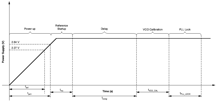 Figure 32. Start-up Time Dependencies
8.3.10 Analog Lock Detect
Figure 33 shows the Analog Lock Detect circuit. Depending upon the phase relationship of the two signals presented at the PFD/CP inputs, the lock detect circuit either charges (if the PLL is locked) or discharges (if PLL is unlocked) the circuit shown via 110μA current sources. An external capacitor determines the sensitivity of the lock detect circuit. The value of the capacitor determines the rate of change of the voltage presented on the output pin PLL_LOCK and hence how quickly the PLL_LOCK output toggles based on a change of PLL locked status. The PLL_LOCK pin is an analog output in analog lock detect mode.

Solving for t yields:

For Example, let:
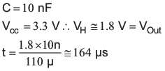
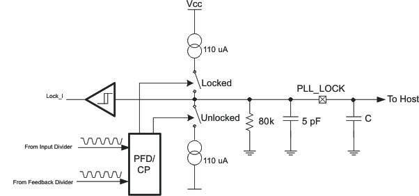 Figure 33. CDCE62005 Analog Lock Detect
8.4 Device Functional Modes
8.4.1 Fan-Out Buffer
Each output of the CDCE62005 can be configured as a fan-out buffer (divider bypassed) or fan-out buffer with divide and skew control functionality.
 Figure 34. CDCE62005 Fan-out Buffer Mode
8.4.2 Clock Generator
The CDCE62005 can generate 5–10 low noise clocks from a single crystal as follows:
 Figure 35. CDCE62005 Clock Generator Mode
8.4.3 Jitter Cleaner – Mixed Mode
The following table presents a common scenario. The CDCE62005 must generate several clocks from a reference that has traversed a backplane. In order for jitter cleaning to take place, the phase noise of the on-board clock path must be better than that of the incoming clock. The designer must pay attention to the optimization of the loop bandwidth of the synthesizer and understand the phase noise profiles of the oscillators involved. Further, other devices on the card require clocks at frequencies not related to the backplane clock. The system requires combinations of differential and single-ended clocks in specific formats with specific phase relationships.
NOTE
Pay special attention when using the universal inputs with two different clock sources. Two clocks derived from the same source may use the internal bias generator and internal termination network without jitter performance degradation. However, if their origin is from different sources ( two independent oscillators, for example) then sharing the internal bias generator can degrade jitter performance significantly.
Table 37. Clock Frequencies
| CLOCK FREQUENCY | INPUT/OUTPUT | FORMAT | NUMBER | CDCE62005 PORT | COMMENT |
|---|---|---|---|---|---|
| 10.000 MHz | Input | LVDS | 1 | SEC_REF | Low end crystal oscillator |
| 30.72 MHz | Input | LVDS | 1 | PRI_REF | Reference from backplane |
| 122.88 MHz | Output | LVDS | 1 | U0 | SERDES Clock |
| 491.52 MHz | Output | LVPECL | 1 | U1 | ASIC |
| 245.76 MHz | Output | LVPECL | 1 | U2 | FPGA |
| 30.72 MHz | Outputs | LVCMOS | 2 | U3 | ASIC |
| 10.000 MHz | Outputs | LVCMOS | 2 | U4 | CPU, DSP |
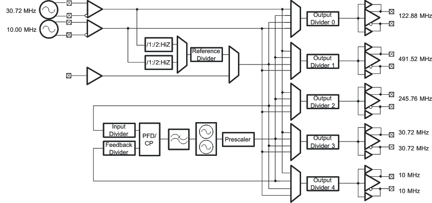 Figure 36. CDCE62005 Jitter Cleaner Example
8.4.3.1 Clocking ADCs with the CDCE62005
High-speed analog to digital converters incorporate high input bandwidth on both the analog port and the sample clock port. Often the input bandwidth far exceeds the sample rate of the converter. Engineers regularly implement receiver chains that take advantage of the characteristics of bandpass sampling. This implementation trend often causes engineers working in communications system design to encounter the term clock limited performance. Therefore, it is important to understand the impact of clock jitter on ADC performance. Equation 14 shows the relationship of data converter signal to noise ratio (SNR) to total jitter.

Total jitter comprises two components: the intrinsic aperture jitter of the converter and the jitter of the sample clock:

With respect to an ADC with N-bits of resolution, ignoring total jitter, DNL, and input noise, the following equation shows the relationship between resolution and SNR:

Figure 37 plots Equation 14 and Equation 16 for constant values of total jitter. When used in conjunction with most ADCs, the CDCE62005 supports a total jitter performance value of <1 ps.
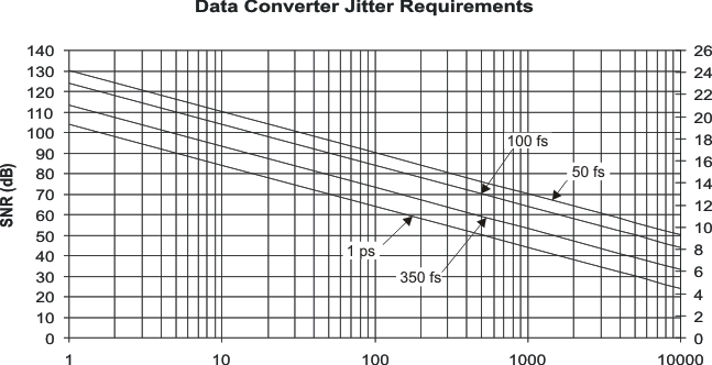 Figure 37. Data Converter Jitter Requirements
8.4.3.2 CDCE62005 SERDES Startup Mode
A common scenario involves a host communicating to a satellite system via a high-speed wired communications link. Typical communications media might be a cable, backplane, or fiber. The reference clock for the satellite system is embedded in the high speed link. This reference clock must be recovered by the SERDES, however, the recovered clock contains unacceptable levels of jitter due to a degradation of SNR associated with transmission over the media. At system startup, the satellite system must self-configure prior to the recovery and cleanup of the reference clock provided by the host. Furthermore, upon loss of the communication link with the host, the satellite system must continue to operate albeit with limited functionality. Figure 38 shows a block diagram of an optical based system with such a mechanism that takes advantage of the features of the CDCE62005:
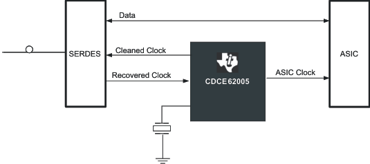 Figure 38. CDCE62005 SERDES Startup Overview
The functionality provided by the Smart Multiplexer provides a straightforward implementation of a SERDES clock link. The Auxiliary Input provides a startup clock because it connects to a crystal. The on-chip EEPROM determines the default configuration at power-up. Therefore, the CDCE62005 requires no host communication to begin cleaning the recovered clock once it is available. The CDCE62005 immediately begins clocking the satellite components including the SERDES using the crystal as a clock source and a frequency reference. After the SERDES recovers the clock, the CDCE62005 removes the jitter via the on-chip synthesizer/loop filter. The recovered clock from the communications link becomes the frequency reference for the satellite system after the smart multiplexer automatically switches over to it. The CDCE62005 applies the cleaned clock to the recovered clock input on the SERDES, thereby establishing a reliable communications link between host and satellite systems.
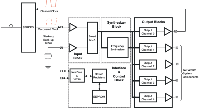 Figure 39. CDCE62005 SERDES Startup Mode
8.5 Programming
8.5.1 Interface and Control Block
The Interface and Control Block includes a SPI interface, three control pins, a non-volatile memory array in which the device stores default configuration data, and an array of device registers implemented in Static RAM. This RAM, also called the device registers, configures all hardware within the CDCE62005.
8.5.1.1 Serial Peripheral Interface (SPI)
The serial interface of CDCE62005 is a simple bidirectional SPI interface for writing and reading to and from the device registers. It implements a low speed serial communications link in a master/slave topology in which the CDCE62005 is a slave. The SPI consists of four signals:
-
SPI_CLK: Serial Clock (Output from Master)
The CDCE62005 clocks data in and out on the rising edge of SPI_CLK. Data transitions therefore occur on the falling edge of the clock.
-
SPI_MOSI: Master Output Slave Input (Output from Master)
-
SPI_MISO: Master Input Slave Output (Output from Slave)
-
SPI_LE: Latch Enable (Output from Master)
The falling edge of SPI_LE initiates a transfer. If SPI_LE is high, no data transfer can take place.
The CDCE62005 implements data fields that are 28-bits wide. In addition, it contains 9 registers, each comprising a 28 bit data field. Therefore, accessing the CDCE62005 requires that the host program append a 4-bit address field to the front of the data field as follows:
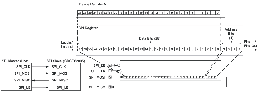 Figure 40. CDCE62005 SPI Communications Format
8.5.1.2 CDCE62005 SPI Command Structure
The CDCE62005 supports four commands issued by the Master via the SPI:
- Write to RAM
- Read Command
- Copy RAM to EEPROM – unlock
- Copy RAM to EEPROM – lock
Table 38 provides a summary of the CDCE62005 SPI command structure. The host (master) constructs a Write to RAM command by specifying the appropriate register address in the address field and appends this value to the beginning of the data field. Therefore, a valid command stream must include 32 bits, transmitted LSB first. The host must issue a Read Command to initiate a data transfer from the CDCE62005 back to the host. This command specifies the address of the register of interest in the data field.
Table 38. CDCE62005 SPI Command Structure
| DATA FIELD (28 Bits) | ADDR FIELD (4 BITS) |
|||||||||||||||||||||||||||||||||
|---|---|---|---|---|---|---|---|---|---|---|---|---|---|---|---|---|---|---|---|---|---|---|---|---|---|---|---|---|---|---|---|---|---|---|
| REGISTER | OPERATION | NVM | 27 | 26 | 25 | 24 | 23 | 22 | 21 | 20 | 19 | 18 | 17 | 16 | 15 | 14 | 13 | 12 | 11 | 10 | 9 | 8 | 7 | 6 | 5 | 4 | 3 | 2 | 1 | 0 | 3 | 2 | 1 | 0 |
| 0 | Write to RAM | Yes | X | X | X | X | X | X | X | X | X | X | X | X | X | X | X | X | X | X | X | X | X | X | X | X | X | X | X | X | 0 | 0 | 0 | 0 |
| 1 | Write to RAM | Yes | X | X | X | X | X | X | X | X | X | X | X | X | X | X | X | X | X | X | X | X | X | X | X | X | X | X | X | X | 0 | 0 | 0 | 1 |
| 2 | Write to RAM | Yes | X | X | X | X | X | X | X | X | X | X | X | X | X | X | X | X | X | X | X | X | X | X | X | X | X | X | X | X | 0 | 0 | 1 | 0 |
| 3 | Write to RAM | Yes | X | X | X | X | X | X | X | X | X | X | X | X | X | X | X | X | X | X | X | X | X | X | X | X | X | X | X | X | 0 | 0 | 1 | 1 |
| 4 | Write to RAM | Yes | X | X | X | X | X | X | X | X | X | X | X | X | X | X | X | X | X | X | X | X | X | X | X | X | X | X | X | X | 0 | 1 | 0 | 0 |
| 5 | Write to RAM | Yes | X | X | X | X | X | X | X | X | X | X | X | X | X | X | X | X | X | X | X | X | X | X | X | X | X | X | X | X | 0 | 1 | 0 | 1 |
| 6 | Write to RAM | Yes | X | X | X | X | X | X | X | X | X | X | X | X | X | X | X | X | X | X | X | X | X | X | X | X | X | X | X | X | 0 | 1 | 1 | 0 |
| 7 | Write to RAM | Yes | X | X | X | X | X | X | X | X | X | X | X | X | X | X | X | X | X | X | X | X | X | X | X | X | X | X | X | X | 0 | 1 | 1 | 1 |
| 8 | Status/Control | No | X | X | X | X | X | X | X | X | X | X | X | X | X | X | X | X | X | X | X | X | X | X | X | X | X | X | X | X | 1 | 0 | 0 | 0 |
| Instruction | Read Command | No | 0 | 0 | 0 | 0 | 0 | 0 | 0 | 0 | 0 | 0 | 0 | 0 | 0 | 0 | 0 | 0 | 0 | 0 | 0 | 0 | 0 | 0 | 0 | 0 | A | A | A | A | 1 | 1 | 1 | 0 |
| Instruction | RAM EEPROM | Unlock | 0 | 0 | 0 | 0 | 0 | 0 | 0 | 0 | 0 | 0 | 0 | 0 | 0 | 0 | 0 | 0 | 0 | 0 | 0 | 0 | 0 | 0 | 0 | 0 | 0 | 0 | 0 | 1 | 1 | 1 | 1 | 1 |
| Instruction | RAM EEPROM | Lock (1) | 0 | 0 | 0 | 0 | 0 | 0 | 0 | 0 | 0 | 0 | 0 | 0 | 0 | 0 | 0 | 0 | 1 | 0 | 1 | 0 | 0 | 0 | 0 | 0 | 0 | 0 | 1 | 1 | 1 | 1 | 1 | 1 |
The CDCE62005 on-board EEPROM has been factory preset to the default settings listed in Table 39.
Table 39. Register and Default Setting
| REGISTER | DEFAULT SETTING |
|---|---|
| REG0000 | 8184032 |
| REG0001 | 8184030 |
| REG0002 | 8186030 |
| REG0003 | EB86030 |
| REG0004 | 0186031 |
| REG0005 | 101C0BE |
| REG0006 | 04BE19A |
| REG0007 | BD0037F |
The Default configurations programmed in the device is set to: Primary and Secondary are set to LVPECL ac-coupled termination and the Auxiliary input is enabled. The Smart Mux is set to auto select among Primary, Secondary and Auxiliary. Reference is set at 25MHz and the dividers are selected to run the VCO at 1875MHz.
- Output 0 & 1 are set to output 156.25MHz with LVPECL signaling
- Output 2 is set to output 125MHz/ LVPECL
- Output 3 is set to output 125MHz/ LVDS
- Output 4 is set to output 125MHz/ LVCMO
8.5.1.3 SPI Interface Master
The Interface master can be designed using a FPGA or a micro controller. The CDCD62005 acts as a slave to the SPI master. The SPI Master should be designed to issue none consecutive read or write commands. The SPI clock should start and stop with respect to the SPI_LE signal as shown in Figure 41. SPI_MOSI, SPI_CLK, and SPI_LE are generated by the SPI Master. SPI_MISO is gnererated by the SPI slave the CDCE62005.
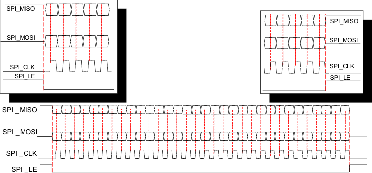 Figure 41. CDCE62005 SPI Read/Write Command
8.5.1.4 SPI Consecutive Read/Write Cycles to the CDCE62005
Figure 42 illustrates how two consecutive SPI cycles are performed between a SPI Master and the CDCE62005 SPI Slave.
 Figure 42. Consecutive Read/Write Cycles
8.5.1.5 Writing to the CDCE62005
Figure 43 illustrates a Write to RAM operation. Notice that the latching of the first data bit in the data stream (Bit 0) occurs on the first rising edge of SPI_CLK after SPI_LE transitions from a high to a low. For the CDCE62005, data transitions occur on the falling edge of SPI_CLK. A rising edge on SPI_LE signals to the CDCE62005 that the transmission of the last bit in the stream (Bit 31) has occurred.
 Figure 43. CDCE62005 SPI Write Operation
8.5.1.6 Reading from the CDCE62005
Figure 44 shows how the CDCE62005 executes a Read Command. The SPI master first issues a Read Command to initiate a data transfer from the CDCE62005 back to the host (see Table 40). This command specifies the address of the register of interest. By transitioning SPI_LE from a low to a high, the CDCE62005 resolves the address specified in the appropriate bits of the data field. The host drives SPI_LE low and the CDCE62005 presents the data present in the register specified in the Read Command on SPI_MISO.
 Figure 44. CDCE62005 Read Operation
8.5.1.7 Writing to EEPROM
After the CDCE62005 detects a power-up and completes a reset cycle, it copies the contents of the on-board EEPROM into the Device Registers. Therefore, the CDCE62005 initializes into a known state pre-defined by the user. The host issues one of two special commands shown in Table 38 to copy the contents of Device Registers 0 through 7 (a total of 184 bits) into EERPOM. They include:
- Copy RAM to EEPROM – Unlock, Execution of this command can happen many times.
- Copy RAM to EEPROM – Lock: Execution of this command can happen only once, after which the EEPROM is permanently locked.
After either command is initiated, power must remain stable and the host must not access the CDCE62005 for at least 50 ms to allow the EEPROM to complete the write cycle and to avoid the possibility of EEPROM corruption.
8.5.2 Device Configuration
The Functional Description Section described four different functional blocks contained within the CDCE62005. Figure 45 depicts these blocks along with a high-level functional block diagram of the circuit elements comprising each block. The balance of this section focuses on a detailed discussion of each functional block from the perspective of how to configure them.
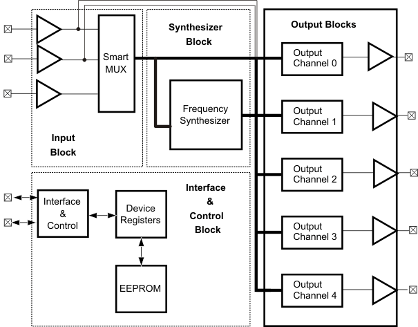 Figure 45. CDCE62005 Circuit Blocks
Throughout this section, references to Device Register memory locations follow the following convention:
 Figure 46. Device Register Reference Convention
8.6 Register Maps
8.6.1 Device Registers: Register 0 Address 0x00
Table 40. CDCE62005 Register 0 Bit Definitions
| RAM BIT | BIT NAME | RELATED BLOCK | DESCRIPTION/FUNCTION | |||||||||
|---|---|---|---|---|---|---|---|---|---|---|---|---|
| 0 | DIV2PRIX | Primary Reference | Pre-Divider Selection for the Primary Reference (X,Y)=00:3-state, 01:Divide by 1, 10:Divide by 2, 11:Reserved |
EEPROM | ||||||||
| 1 | DIV2PRIY | EEPROM | ||||||||||
| 2 | RESERVED | Must be set to 0 | EEPROM | |||||||||
| 3 | RESERVED | Must be set to 0 | EEPROM | |||||||||
| 4 | OUTMUX0SELX | Output 0 | OUTPUT MUX 0 Select. Selects the Signal driving Output Divider 0 (X,Y) = 00: PRI_REF, 01:SEC_REF, 10:SMART_MUX, 11:VCO_CORE |
EEPROM | ||||||||
| 5 | OUTMUX0SELY | Output 0 | EEPROM | |||||||||
| 6 | PH0ADJC0 | Output 0 | Coarse phase adjust select for output divider 0 | EEPROM | ||||||||
| 7 | PH0ADJC1 | Output 0 | EEPROM | |||||||||
| 8 | PH0ADJC2 | Output 0 | EEPROM | |||||||||
| 9 | PH0ADJC3 | Output 0 | EEPROM | |||||||||
| 10 | PH0ADJC4 | Output 0 | EEPROM | |||||||||
| 11 | PH0ADJC5 | Output 0 | EEPROM | |||||||||
| 12 | PH0ADJC6 | Output 0 | EEPROM | |||||||||
| 13 | OUT0DIVRSEL0 | Output 0 | OUTPUT DIVIDER 0 Ratio Select | EEPROM | ||||||||
| 14 | OUT0DIVRSEL1 | Output 0 | EEPROM | |||||||||
| 15 | OUT0DIVRSEL2 | Output 0 | EEPROM | |||||||||
| 16 | OUT0DIVRSEL3 | Output 0 | EEPROM | |||||||||
| 17 | OUT0DIVRSEL4 | Output 0 | EEPROM | |||||||||
| 18 | OUT0DIVRSEL5 | Output 0 | EEPROM | |||||||||
| 19 | OUT0DIVRSEL6 | Output 0 | EEPROM | |||||||||
| 20 | OUT0DIVSEL | Output 0 | When set to 0, the divider is disabled. When set to 1, the divider is enabled. |
EEPROM | ||||||||
| 21 | HiSWINGLVPECL0 | Output 0 | High Swing LVPECL When set to 1 and Normal Swing when set to 0. – If LVCMOS or LVDS is selected the Output swing will stay at the same level.(1) – If LVPECL buffer is selected the Output Swing will be 30% higher if this bit is set to 1 and Normal LVPECL if it is set to 0. |
EEPROM | ||||||||
| 22 | CMOSMODE0PX | Output 0 | LVCMOS mode select for OUTPUT 0 Positive Pin. (X,Y)=00:Active, 10:Inverting, 11:Low, 01:3-State |
EEPROM | ||||||||
| 23 | CMOSMODE0PY | Output 0 | EEPROM | |||||||||
| 24 | CMOSMODE0NX | Output 0 | LVCMOS mode select for OUTPUT 0 Negative Pin. (X,Y)=00:Active, 10:Inverting, 11:Low, 01:3-State |
EEPROM | ||||||||
| 25 | CMOSMODE0NY | Output 0 | EEPROM | |||||||||
| 26 | OUTBUFSEL0X | Output 0 | OUTPUT TYPE | RAM BITS | EEPROM | |||||||
| 27 | OUTBUFSEL0Y | Output 0 | 22 | 23 | 24 | 25 | 26 | 27 | EEPROM | |||
| LVPECL | 0 | 0 | 0 | 0 | 0 | 1 | ||||||
| LVDS | 0 | 1 | 0 | 1 | 1 | 1 | ||||||
| LVCMOS | See Settings Above | 0 | 0 | |||||||||
| Output Disabled | 0 | 1 | 0 | 1 | 1 | 0 | ||||||
| * Use Description for Bits 22,23,24 and 25 for setting the LVCMOS Outputs | ||||||||||||
8.6.2 Device Registers: Register 1 Address 0x01
Table 41. CDCE62005 Register 1 Bit Definitions
| RAM BIT | BIT NAME | RELATED BLOCK | DESCRIPTION/FUNCTION | |||||||||
|---|---|---|---|---|---|---|---|---|---|---|---|---|
| 0 | DIV2SECX | Secondary Reference | Pre-Divider Selection for the Secondary Reference (X,Y)=00:3-state, 01:Divide by 1, 10:Divide by 2, 11:Reserved |
EEPROM | ||||||||
| 1 | DIV2SECY | EEPROM | ||||||||||
| 2 | RESERVED | Must be set to 0 | EEPROM | |||||||||
| 3 | RESERVED | Must be set to 0 | EEPROM | |||||||||
| 4 | OUTMUX1SELX | Output 1 | OUTPUT MUX 1 Select. Selects the Signal driving Output Divider 1. (X,Y) = 00: PRI_REF, 01:SEC_REF, 10:SMART_MUX, 11:VCO_CORE |
EEPROM | ||||||||
| 5 | OUTMUX1SELY | Output 1 | EEPROM | |||||||||
| 6 | PH1ADJC0 | Output 1 | Coarse phase adjust select for output divider 1 | EEPROM | ||||||||
| 7 | PH1ADJC1 | Output 1 | EEPROM | |||||||||
| 8 | PH1ADJC2 | Output 1 | EEPROM | |||||||||
| 9 | PH1ADJC3 | Output 1 | EEPROM | |||||||||
| 10 | PH1ADJC4 | Output 1 | EEPROM | |||||||||
| 11 | PH1ADJC5 | Output 1 | EEPROM | |||||||||
| 12 | PH1ADJC6 | Output 1 | EEPROM | |||||||||
| 13 | OUT1DIVRSEL0 | Output 1 | OUTPUT DIVIDER 1 Ratio Select | EEPROM | ||||||||
| 14 | OUT1DIVRSEL1 | Output 1 | EEPROM | |||||||||
| 15 | OUT1DIVRSEL2 | Output 1 | EEPROM | |||||||||
| 16 | OUT1DIVRSEL3 | Output 1 | EEPROM | |||||||||
| 17 | OUT1DIVRSEL4 | Output 1 | EEPROM | |||||||||
| 18 | OUT1DIVRSEL5 | Output 1 | EEPROM | |||||||||
| 19 | OUT1DIVRSEL6 | Output 1 | EEPROM | |||||||||
| 20 | OUT1DIVSEL | Output 1 | When set to 0, the divider is disabled When set to 1, the divider is enabled |
EEPROM | ||||||||
| 21 | HiSWINGLVPECL1 | Output 1 | High Swing LVPECL When set to 1 and Normal Swing when set to 0 – If LVCMOS or LVDS is selected the Output swing will stay at the same level.(1) – If LVPECL buffer is selected the Output Swing will be 30% higher if this bit is set to 1 and Normal LVPECL if it is set to 0. |
EEPROM | ||||||||
| 22 | CMOSMODE1PX | Output 1 | LVCMOS mode select for OUTPUT 1 Positive Pin. (X,Y)=00:Active, 10:Inverting, 11:Low, 01:3-State |
EEPROM | ||||||||
| 23 | CMOSMODE1PY | Output 1 | EEPROM | |||||||||
| 24 | CMOSMODE1NX | Output 1 | LVCMOS mode select for OUTPUT 1 Negative Pin. (X,Y)=00:Active, 10:Inverting, 11:Low, 01:3-State |
EEPROM | ||||||||
| 25 | CMOSMODE1NY | Output 1 | EEPROM | |||||||||
| 26 | OUTBUFSEL1X | Output 1 | OUTPUT TYPE | RAM BITS | EEPROM | |||||||
| 27 | OUTBUFSEL1Y | Output 1 | 22 | 23 | 24 | 25 | 26 | 27 | EEPROM | |||
| LVPECL | 0 | 0 | 0 | 0 | 0 | 1 | ||||||
| LVDS | 0 | 1 | 0 | 1 | 1 | 1 | ||||||
| LVCMOS | See Settings Above* | 0 | 0 | |||||||||
| Output Disabled | 0 | 1 | 0 | 1 | 1 | 0 | ||||||
| * Use Description for Bits 22,23,24 and 25 for setting the LVCMOS Outputs | ||||||||||||
8.6.3 Device Registers: Register 2 Address 0x02
Table 42. CDCE62005 Register 2 Bit Definitions
| RAM BIT | BIT NAME | RELATED BLOCK | DESCRIPTION/FUNCTION | |||||||||
|---|---|---|---|---|---|---|---|---|---|---|---|---|
| 0 | REFDIV0 | Reference Divider | Reference Divider Bit 0 | EEPROM | ||||||||
| 1 | REFDIV1 | Reference Divider Bit 1 | EEPROM | |||||||||
| 2 | RESERVED | Must be set to 0 | EEPROM | |||||||||
| 3 | RESERVED | Must be set to 0 | EEPROM | |||||||||
| 4 | OUTMUX2SELX | Output 2 | OUTPUT MUX 2 Select. Selects the Signal driving Output Divider 2 (X,Y) = 00: PRI_REF, 01:SEC_REF, 10:SMART_MUX, 11:VCO_CORE |
EEPROM | ||||||||
| 5 | OUTMUX2SELY | Output 2 | EEPROM | |||||||||
| 6 | PH2ADJC0 | Output 2 | Coarse phase adjust select for output divider 2 | EEPROM | ||||||||
| 7 | PH2ADJC1 | Output 2 | EEPROM | |||||||||
| 8 | PH2ADJC2 | Output 2 | EEPROM | |||||||||
| 9 | PH2ADJC3 | Output 2 | EEPROM | |||||||||
| 10 | PH2ADJC4 | Output 2 | EEPROM | |||||||||
| 11 | PH2ADJC5 | Output 2 | EEPROM | |||||||||
| 12 | PH2ADJC6 | Output 2 | EEPROM | |||||||||
| 13 | OUT2DIVRSEL0 | Output 2 | OUTPUT DIVIDER 2 Ratio Select | EEPROM | ||||||||
| 14 | OUT2DIVRSEL1 | Output 2 | EEPROM | |||||||||
| 15 | OUT2DIVRSEL2 | Output 2 | EEPROM | |||||||||
| 16 | OUT2DIVRSEL3 | Output 2 | EEPROM | |||||||||
| 17 | OUT2DIVRSEL4 | Output 2 | EEPROM | |||||||||
| 18 | OUT2DIVRSEL5 | Output 2 | EEPROM | |||||||||
| 19 | OUT2DIVRSEL6 | Output 2 | EEPROM | |||||||||
| 20 | OUT2DIVSEL | Output 2 | When set to 0, the divider is disabled When set to 1, the divider is enabled |
EEPROM | ||||||||
| 21 | HiSWINGLVPEC2 | Output 2 | High Swing LVPECL When set to 1 and Normal Swing when set to 0. – If LVCMOS or LVDS is selected the Output swing will stay at the same level.(1) – If LVPECL buffer is selected the Output Swing will be 30% higher if this bit is set to 1 and Normal LVPECL if it is set to 0. |
EEPROM | ||||||||
| 22 | CMOSMODE2PX | Output 2 | LVCMOS mode select for OUTPUT 2 Positive Pin. (X,Y)=00:Active, 10:Inverting, 11:Low, 01:3-State |
EEPROM | ||||||||
| 23 | CMOSMODE2PY | Output 2 | EEPROM | |||||||||
| 24 | CMOSMODE2NX | Output 2 | LVCMOS mode select for OUTPUT 2 Negative Pin. (X,Y)=00:Active, 10:Inverting, 11:Low, 01:3-State |
EEPROM | ||||||||
| 25 | CMOSMODE2NY | Output 2 | EEPROM | |||||||||
| 26 | OUTBUFSEL2X | Output 2 | OUTPUT TYPE | RAM BITS | EEPROM | |||||||
| 27 | OUTBUFSEL2Y | Output 2 | 22 | 23 | 24 | 25 | 26 | 27 | EEPROM | |||
| LVPECL | 0 | 0 | 0 | 0 | 0 | 1 | ||||||
| LVDS | 0 | 1 | 0 | 1 | 1 | 1 | ||||||
| LVCMOS | See Settings Above | 0 | 0 | |||||||||
| Output Disabled | 0 | 1 | 0 | 1 | 1 | 0 | ||||||
| * Use Description for Bits 22,23,24 and 25 for setting the LVCMOS Outputs | ||||||||||||
8.6.4 Device Registers: Register 3 Address 0x03
Table 43. CDCE62005 Register 3 Bit Definitions
| RAM BIT | BIT NAME | RELATED BLOCK | DESCRIPTION/FUNCTION | |||||||||
|---|---|---|---|---|---|---|---|---|---|---|---|---|
| 0 | REFDIV2 | Reference Divider | Reference Divider Bit 2. | EEPROM | ||||||||
| 1 | RESERVED | Must be set to 0. | EEPROM | |||||||||
| 2 | RESERVED | Must be set to 0. | EEPROM | |||||||||
| 3 | RESERVED | Must be set to 0. | EEPROM | |||||||||
| 4 | OUTMUX3SELX | Output 3 | OUTPUT MUX 3 Select. Selects the Signal driving Output Divider 3. (X,Y) = 00: PRI_REF, 01:SEC_REF, 10:SMART_MUX, 11:VCO_CORE |
EEPROM | ||||||||
| 5 | OUTMUX3SELY | Output 3 | EEPROM | |||||||||
| 6 | PH3ADJC0 | Output 3 | Coarse phase adjust select for output divider 3 | EEPROM | ||||||||
| 7 | PH3ADJC1 | Output 3 | EEPROM | |||||||||
| 8 | PH3ADJC2 | Output 3 | EEPROM | |||||||||
| 9 | PH3ADJC3 | Output 3 | EEPROM | |||||||||
| 10 | PH3ADJC4 | Output 3 | EEPROM | |||||||||
| 11 | PH3ADJC5 | Output 3 | EEPROM | |||||||||
| 12 | PH3ADJC6 | Output 3 | EEPROM | |||||||||
| 13 | OUT3DIVRSEL0 | Output 3 | OUTPUT DIVIDER 3 Ratio Select | EEPROM | ||||||||
| 14 | OUT3DIVRSEL1 | Output 3 | EEPROM | |||||||||
| 15 | OUT3DIVRSEL2 | Output 3 | EEPROM | |||||||||
| 16 | OUT3DIVRSEL3 | Output 3 | EEPROM | |||||||||
| 17 | OUT3DIVRSEL4 | Output 3 | EEPROM | |||||||||
| 18 | OUT3DIVRSEL5 | Output 3 | EEPROM | |||||||||
| 19 | OUT3DIVRSEL6 | Output 3 | EEPROM | |||||||||
| 20 | OUT3DIVSEL | Output 3 | When set to 0, the divider is disabled When set to 1, the divider is enabled |
EEPROM | ||||||||
| 21 | HiSWINGLVPEC3 | Output 3 | High Swing LVPECL When set to 1 and Normal Swing when set to 0. – If LVCMOS or LVDS is selected the Output swing will stay at the same level.(1). – If LVPECL buffer is selected the Output Swing will be 30% higher if this bit is set to 1 and Normal LVPECL if it is set to 0. |
EEPROM | ||||||||
| 22 | CMOSMODE3PX | Output 3 | LVCMOS mode select for OUTPUT 3 Positive Pin. (X,Y)=00:Active, 10:Inverting, 11:Low, 01:3-State |
EEPROM | ||||||||
| 23 | CMOSMODE3PY | Output 3 | EEPROM | |||||||||
| 24 | CMOSMODE3NX | Output 3 | LVCMOS mode select for OUTPUT 3 Negative Pin. (X,Y)=00:Active, 10:Inverting, 11:Low, 01:3-State |
EEPROM | ||||||||
| 25 | CMOSMODE3NY | Output 3 | EEPROM | |||||||||
| 26 | OUTBUFSEL3X | Output 3 | OUTPUT TYPE | RAM BITS | EEPROM | |||||||
| 27 | OUTBUFSEL3Y | Output 3 | 22 | 23 | 24 | 25 | 26 | 27 | EEPROM | |||
| LVPECL | 0 | 0 | 0 | 0 | 0 | 1 | ||||||
| LVDS | 0 | 1 | 0 | 1 | 1 | 1 | ||||||
| LVCMOS | See Settings Above* | 0 | 0 | |||||||||
| Output Disabled | 0 | 1 | 0 | 1 | 1 | 0 | ||||||
| * Use Description for Bits 22,23,24 and 25 for setting the LVCMOS Outputs | ||||||||||||
8.6.5 Device Registers: Register 4 Address 0x04
Table 44. CDCE62005 Register 4 Bit Definitions
| RAM BIT | BIT NAME | RELATED BLOCK | DESCRIPTION/FUNCTION | |||||||||
|---|---|---|---|---|---|---|---|---|---|---|---|---|
| 0 | RESERVED | — | This bit must be set to a 1 | EEPROM | ||||||||
| 1 | SYNC_MODE1 | Outputs | 0 (default): Outputs have deterministic delay relative to low-to-high pulse of SYNC pin when the EEPROM SYNC signal is synchronized with the reference input and added 6μs delay. 1: outputs have deterministic delay relative to low-to-high pulse of SYNC pin when the SYNC signal is synchronized with the reference input |
EEPROM | ||||||||
| 2 | RESERVED | Must be set to 0 | EEPROM | |||||||||
| 3 | RESERVED | Must be set to 0 | EEPROM | |||||||||
| 4 | OUTMUX4SELX | Output 4 | OUTPUT MUX 4 Select. Selects the Signal driving Output Divider 4 (X,Y) = 00: PRI_REF, 01:SEC_REF, 10:SMART_MUX, 11:VCO_CORE |
EEPROM | ||||||||
| 5 | OUTMUX4SELY | Output 4 | EEPROM | |||||||||
| 6 | PH4ADJC0 | Output 4 | Coarse phase adjust select for output divider 4 | EEPROM | ||||||||
| 7 | PH4ADJC1 | Output 4 | EEPROM | |||||||||
| 8 | PH4ADJC2 | Output 4 | EEPROM | |||||||||
| 9 | PH4ADJC3 | Output 4 | EEPROM | |||||||||
| 10 | PH4ADJC4 | Output 4 | EEPROM | |||||||||
| 11 | PH4ADJC5 | Output 4 | EEPROM | |||||||||
| 12 | PH4ADJC6 | Output 4 | EEPROM | |||||||||
| 13 | OUT4DIVRSEL0 | Output 4 | OUTPUT DIVIDER 4 Ratio Select | EEPROM | ||||||||
| 14 | OUT4DIVRSEL1 | Output 4 | EEPROM | |||||||||
| 15 | OUT4DIVRSEL2 | Output 4 | EEPROM | |||||||||
| 16 | OUT4DIVRSEL3 | Output 4 | EEPROM | |||||||||
| 17 | OUT4DIVRSEL4 | Output 4 | EEPROM | |||||||||
| 18 | OUT4DIVRSEL5 | Output 4 | EEPROM | |||||||||
| 19 | OUT4DIVRSEL6 | Output 4 | EEPROM | |||||||||
| 20 | OUT4DIVSEL | Output 4 | When set to 0, the divider is disabled When set to 1, the divider is enabled |
EEPROM | ||||||||
| 21 | HiSWINGLVPEC4 | Output 4 | High Swing LVPECL When set to 1 and Normal Swing when set to 0. – If LVCMOS or LVDS is selected the Output swing will stay at the same level.(1) – If LVPECL buffer is selected the Output Swing will be 30% higher if this bit is set to 1 and Normal LVPECL if it is set to 0. |
EEPROM | ||||||||
| 22 | CMOSMODE4PX | Output 4 | LVCMOS mode select for OUTPUT 4 Positive Pin. (X,Y)=00:Active, 10:Inverting, 11:Low, 01:3-State |
EEPROM | ||||||||
| 23 | CMOSMODE4PY | Output 4 | EEPROM | |||||||||
| 24 | CMOSMODE4NX | Output 4 | LVCMOS mode select for OUTPUT 3 Negative Pin. (X,Y)=00:Active, 10:Inverting, 11:Low, 01:3-State |
EEPROM | ||||||||
| 25 | CMOSMODE4NY | Output 4 | EEPROM | |||||||||
| 26 | OUTBUFSEL4X | Output 4 | OUTPUT TYPE | RAM BITS | EEPROM | |||||||
| 27 | OUTBUFSEL4Y | Output 4 | 22 | 23 | 24 | 25 | 26 | 27 | EEPROM | |||
| LVPECL | 0 | 0 | 0 | 0 | 0 | 1 | ||||||
| LVDS | 0 | 1 | 0 | 1 | 1 | 1 | ||||||
| LVCMOS | See Settings Above* | 0 | 0 | |||||||||
| Output Disabled | 0 | 1 | 0 | 1 | 1 | 0 | ||||||
| * Use Description for Bits 22,23,24 and 25 for setting the LVCMOS Outputs | ||||||||||||
8.6.6 Device Registers: Register 5 Address 0x05
Table 45. CDCE62005 Register 5 Bit Definitions
| RAM BIT | BIT NAME | RELATED BLOCK | DESCRIPTION/FUNCTION | |
|---|---|---|---|---|
| 0 | INBUFSELX | INBUFSELX | Input Buffer Select (LVPECL,LVDS or LVCMOS) Reg5[1:0]=00=LVCMOS Reg5[1:0]=01=reserved Reg5[1:0]=10=LVPECL Reg5[1:0]=11=LVDS |
EEPROM |
| 1 | INBUFSELY | INBUFSELY | EEPROM | |
| 2 | PRISEL | Smart MUX | When EECLKSEL = 1; Bit (2,3,4) 100 – PRISEL, 010 – SECSEL , 001 – AUXSEL 110 – Auto Select (PRI then SEC) 111 – Auto Select (PRI then SEC and then AUX) When EECLKSEL = 0, REF_SEL pin determines the Reference Input to the Smart Mux circuitry. |
EEPROM |
| 3 | SECSEL | EEPROM | ||
| 4 | AUXSEL(1) | EEPROM | ||
| 5 | EECLKSEL | Smart MUX | If EEPROM Clock Select Input is set to 1 The Clock selections follows internal EEPROM settings and ignores REF_SEL Pin status, when Set to 0 REF_SEL is used to control the Mux, Auto Select Function is not available and AUXSEL is not available. | EEPROM |
| 6 | ACDCSEL | Input Buffers | If set to 1 DC Termination, If set to 0 AC Termination | EEPROM |
| 7 | HYSTEN | Input Buffers | If set to 1 Input Buffers Hysteresis Enabled. It is not recommended that Hysteresis be disabled. | EEPROM |
| 8 | PRI_TERMSEL | Input Buffers | If set to 0 Primary Input Buffer Internal Termination Enabled If set to 1 Primary Internal Termination circuitry Disabled |
EEPROM |
| 9 | PRIINVBB | Input Buffers | If set to 0 Primary Input Negative Pin Biased with Internal VBB Voltage. | EEPROM |
| 10 | SECINVBB | Input Buffers | If set to 0 Secondary Input Negative Pin Biased with Internal VBB Voltage | EEPROM |
| 11 | FAILSAFE | Input Buffers | If set to 1 Fail Safe is Enabled for all Input Buffers configured as LVDS, DC Coupling only. | EEPROM |
| 12 | RESERVED | Must be set to 0 | EEPROM | |
| 13 | RESERVED | Must be set to 0 | EEPROM | |
| 14 | SELINDIV0 | VCO Core | INPUT DIVIDER Settings | EEPROM |
| 15 | SELINDIV1 | VCO Core | EEPROM | |
| 16 | SELINDIV2 | VCO Core | EEPROM | |
| 17 | SELINDIV3 | VCO Core | EEPROM | |
| 18 | SELINDIV4 | VCO Core | EEPROM | |
| 19 | SELINDIV5 | VCO Core | EEPROM | |
| 20 | SELINDIV6 | VCO Core | EEPROM | |
| 21 | SELINDIV7 | VCO Core | EEPROM | |
| 22 | LOCKW(0) | PLL Lock | See Table 34 | EEPROM |
| 23 | LOCKW(1) | EEPROM | ||
| 24 | LOCKW(2) | EEPROM | ||
| 25 | LOCKW(3) | EEPROM | ||
| 26 | LOCKDET | PLL Lock | Number of coherent lock events. If set to 0 it triggers after the first lock detection if set to 1 it triggers lock after 64 PFD cycles of lock detections. | EEPROM |
| 27 | ADLOCK | PLL Lock | Selects Digital PLL_LOCK 0 ,Selects Analog PLL_LOCK 1 | EEPROM |
8.6.7 Device Registers: Register 6 Address 0x06
Table 46. CDCE62005 Register 6 Bit Definitions
| RAM BIT | BIT NAME | RELATED BLOCK | DESCRIPTION/FUNCTION | |
|---|---|---|---|---|
| 0 | SELVCO | VCO Core | VCO Select, 0:VCO1(low range), 1:VCO2(high range) | EEPROM |
| 1 | SELPRESCA | VCO Core | PRESCALER Setting. | EEPROM |
| 2 | SELPRESCB | VCO Core | EEPROM | |
| 3 | SELFBDIV0 | VCO Core | FEEDBACK DIVIDER Setting | EEPROM |
| 4 | SELFBDIV1 | VCO Core | EEPROM | |
| 5 | SELFBDIV2 | VCO Core | EEPROM | |
| 6 | SELFBDIV3 | VCO Core | EEPROM | |
| 7 | SELFBDIV4 | VCO Core | EEPROM | |
| 8 | SELFBDIV5 | VCO Core | EEPROM | |
| 9 | SELFBDIV6 | VCO Core | EEPROM | |
| 10 | SELFBDIV7 | VCO Core | EEPROM | |
| 11 | RESERVED | Must be set to 0 | EEPROM | |
| 12 | SEC_TERMSEL | Input Buffers | If Set to Secondary Input Buffer Internal Termination Enabled If set to 1 Secondary Internal Termination circuitry Disabled |
EEPROM |
| 13 | SELBPDIV0 | VCO Core | BYPASS DIVIDER Setting (6 settings + Disable + Enable) | EEPROM |
| 14 | SELBPDIV1 | VCO Core | EEPROM | |
| 15 | SELBPDIV2 | VCO Core | EEPROM | |
| 16 | ICPSEL0 | VCO Core | CHARGE PUMP Current Select (see Table 27) | EEPROM |
| 17 | ICPSEL1 | VCO Core | EEPROM | |
| 18 | ICPSEL2 | VCO Core | EEPROM | |
| 19 | ICPSEL3 | VCO Core | EEPROM | |
| 20 | SYNC_MODE2 | VCO Core | When set to 0, outputs are synchronized to the reference input on the low-to-high pulse on SYNC pin or bit. When set to 1, outputs are synchronized to the SYNC low-to-high pulse | EEPROM |
| 21 | CPPULSEWIDTH | VCO Core | If set to 1=wide pulse, 0=narrow pulse | EEPROM |
| 22 | ENCAL | VCO Core | Enable VCO Calibration Command. To execute this command a rising edge must be generated (that is, Write a LOW followed by a high to this bit location). This will initiate a VCO calibration sequence only if Calibration Mode = Manual Mode (that is, Register 6 bit 27 is HIGH). | EEPROM |
| 23 | RESERVED | Must be set to 0 | EEPROM | |
| 24 | AUXOUTEN | Output AUX | Enable Auxiliary Output when set to 1. | EEPROM |
| 25 | AUXFEEDSEL | Output AUX | Select the Output that will driving the AUX Output; Low for Selecting Output Divider 2 and High for Selecting Output Divider 3 |
EEPROM |
| 26 | EXLFSEL | VCO Core | When Set to 1 External Loop filter is used. When Set to 0 Internal Loop Filter is used. |
EEPROM |
| 27 | ENCAL_MODE | PLL Calibration | 1: Calibration Mode = Manual Mode. In this mode, a calibration will be initiated if a rising edge is asserted on ENCAL (Register 6 Bit 22). 0: Calibration Mode = Startup Mode. |
EEPROM |
8.6.8 Device Registers: Register 7 Address 0x07
Table 47. CDCE62005 Register 7 Bit Definitions
| RAM BIT | BIT NAME | RELATED BLOCK | DESCRIPTION/FUNCTION | |
|---|---|---|---|---|
| 0 | LFRCSEL0 | VCO Core | Loop Filter Control Setting | EEPROM |
| 1 | LFRCSEL1 | VCO Core | Loop Filter Control Setting | EEPROM |
| 2 | LFRCSEL2 | VCO Core | Loop Filter Control Setting | EEPROM |
| 3 | LFRCSEL3 | VCO Core | Loop Filter Control Setting | EEPROM |
| 4 | LFRCSEL4 | VCO Core | Loop Filter Control Setting | EEPROM |
| 5 | LFRCSEL5 | VCO Core | Loop Filter Control Setting | EEPROM |
| 6 | LFRCSEL6 | VCO Core | Loop Filter Control Setting | EEPROM |
| 7 | LFRCSEL7 | VCO Core | Loop Filter Control Setting | EEPROM |
| 8 | LFRCSEL8 | VCO Core | Loop Filter Control Setting | EEPROM |
| 9 | LFRCSEL9 | VCO Core | Loop Filter Control Setting | EEPROM |
| 10 | LFRCSEL10 | VCO Core | Loop Filter Control Setting | EEPROM |
| 11 | LFRCSEL11 | VCO Core | Loop Filter Control Setting | EEPROM |
| 12 | LFRCSEL12 | VCO Core | Loop Filter Control Setting | EEPROM |
| 13 | LFRCSEL13 | VCO Core | Loop Filter Control Setting | EEPROM |
| 14 | LFRCSEL14 | VCO Core | Loop Filter Control Setting | EEPROM |
| 15 | LFRCSEL15 | VCO Core | Loop Filter Control Setting | EEPROM |
| 16 | LFRCSEL16 | VCO Core | Loop Filter Control Setting | EEPROM |
| 17 | LFRCSEL17 | VCO Core | Loop Filter Control Setting | EEPROM |
| 18 | LFRCSEL18 | VCO Core | Loop Filter Control Setting | EEPROM |
| 19 | LFRCSEL19 | VCO Core | Loop Filter Control Setting | EEPROM |
| 20 | LFRCSEL20 | VCO Core | Loop Filter Control Setting | EEPROM |
| 21 | RESERVED | Must be set to 0 | EEPROM | |
| 22 | RESERVED | Must be set to 1 | EEPROM | |
| 23 | SEL_DEL2 | Smart Mux | If set to 0, it enables short delay for fast operation If Set to 1, Long Delay recommended for Input References below 150 MHz. |
EEPROM |
| 24 | RESERVED | Must be set to 1 | EEPROM | |
| 25 | SEL_DEL1 | Smart Mux | If set to 0, it enables short delay for fast operation If Set to 1, Long Delay recommended for Input References below 150 MHz. |
EEPROM |
| 26 | EPLOCK | Status | Read Only If EPLOCK reads 0 EEPROM is unlocked. If EPLOCK reads 1, then the EEPROM is locked (see Table 38 for how to lock the EEPROM – this can only be executed once after which the EEPROM is locked permanently). |
EEPROM |
| 27 | RESERVED | Status | Read Only; Always reads 1. | EEPROM |
8.6.9 Device Registers: Register 8 Address 0x08
Table 48. CDCE62005 Register 8 Bit Definitions
| RAM BIT | BIT NAME | RELATED BLOCK | DESCRIPTION/FUNCTION | |
|---|---|---|---|---|
| 0 | CALWORD0 | Status | VCO Calibration Word read back from device (Read only) | RAM |
| 1 | CALWORD1 | Status | RAM | |
| 2 | CALWORD2 | Status | RAM | |
| 3 | CALWORD3 | Status | RAM | |
| 4 | CALWORD4 | Status | RAM | |
| 5 | CALWORD5 | Status | RAM | |
| 6 | PLLLOCKPIN | Status | Read Only: Status of the PLL Lock Pin Driven by the device. | RAM |
| 7 | SLEEP | Control | Set Device Sleep mode On when set to 0, Normal Mode when set to 1 | RAM |
| 8 | SYNC | Control | If set to 0 this bit forces /SYNC; Set to 1 to exit the Synchronization State. | RAM |
| 9 | RESERVED | Must be set to 0 | RAM | |
| 10 | VERSION0 | Read only | RAM | |
| 11 | VERSION1 | Read only | RAM | |
| 12 | VERSION2 | Read only | RAM | |
| 13 | RESERVED | Must be set to 0 | RAM | |
| 14 | CALWORD_IN0 | Diagnostics | TI Test Registers. For TI Use Only (Must be set to 0) | RAM |
| 15 | CALWORD_IN1 | Diagnostics | RAM | |
| 16 | CALWORD_IN2 | Diagnostics | RAM | |
| 17 | CALWORD_IN3 | Diagnostics | RAM | |
| 18 | CALWORD_IN4 | Diagnostics | RAM | |
| 19 | CALWORD_IN5 | Diagnostics | RAM | |
| 20 | RESERVED | Must be set to 0 | RAM | |
| 21 | TITSTCFG0 | Diagnostics | TI Test Registers. For TI Use Only (Must be set to 0) | RAM |
| 22 | TITSTCFG1 | Diagnostics | RAM | |
| 23 | TITSTCFG2 | Diagnostics | RAM | |
| 24 | TITSTCFG3 | Diagnostics | RAM | |
| 25 | PRIACTIVITY | Status | Synthesizer Source Indicator (27:25) (Read only) 0 0 1 Primary Input 0 1 0 Secondary Input 1 0 0 Auxiliary Input |
RAM |
| 26 | SECACTIVITY | Status | RAM | |
| 27 | AUXACTIVITY | Status | RAM |
