ZHCSQA3F November 1997 – March 2022 CD54HC4094 , CD74HC4094 , CD74HCT4094
PRODUCTION DATA
- 1 特性
- 2 说明
- 3 Revision History
- 4 Pin Configuration and Functions
- 5 Specifications
- 6 Parameter Measurement Information
- 7 Detailed Description
- 8 Power Supply Recommendations
- 9 Layout
- 10Device and Documentation Support
- 11Mechanical, Packaging, and Orderable Information
封装选项
请参考 PDF 数据表获取器件具体的封装图。
机械数据 (封装 | 引脚)
- PW|16
- DYY|16
- NS|16
- N|16
- D|16
散热焊盘机械数据 (封装 | 引脚)
订购信息
6 Parameter Measurement Information
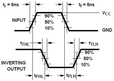
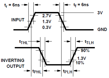
tPD is the maximum between tPLH and tPHL
tt is the maximum between tTLH and tTHL
 Figure 6-1 HC and HCT transition times and
propagation delay times, combination logic
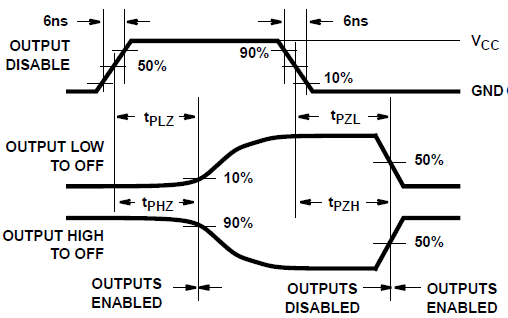
 Figure 6-3 HC three-state propagation delay
waveform
NOTE: Open drain waveforms tPLZ and tPZL are the same as those for three-state shown on the left. The test circuit is Output RL = 1kΩ to VCC, CL = 50pF.
Figure 6-5 HC and HCT three-state propagation delay test circuit Figure 6-2 HCT transition times and tpopationg
delay times, combination logic
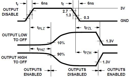
 Figure 6-4 HCT three-state propagation delay
waveform