ZHCSCJ7E July 2013 – June 2014 CC3200
PRODUCTION DATA.
- 1器件概述
- 2修订历史记录
- 3Terminal Configuration and Functions
- 4Specifications
- 5Detailed Description
- 6Applications and Implementation
- 7器件和文档支持
- 8机械封装和可订购信息
5 Detailed Description
5.1 Overview
The CC3200 device has a rich set of peripherals for diverse application requirements. The device optimizes bus matrix and memory management to give the application developer the needed advantage. This section briefly highlights the internal details of the CC3200 device and offers suggestions for application configurations.
5.1.1 Device Features
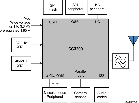
5.2 Functional Block Diagram
Figure 5-1 shows the functional block diagram of the CC3200 SimpleLink Wi-Fi solution.
5.3 ARM Cortex-M4 Processor Core Subsystem
The high-performance ARM Cortex-M4 processor provides a low-cost platform that meets the needs of minimal memory implementation, reduced pin count, and low power consumption, while delivering outstanding computational performance and exceptional system response to interrupts.
- The ARM Cortex-M4 core has low-latency interrupt processing with the following features:
- A 32-bit ARM Cortex Thumb® instruction set optimized for embedded applications
- Handler and thread modes
- Low-latency interrupt handling by automatic processor state saving and restoration during entry and exit
- Support for ARMv6 unaligned accesses
- Nested vectored interrupt controller (NVIC) closely integrated with the processor core to achieve low latency interrupt processing. Features include:
- Bits of priority configurable from 3 to 8
- Dynamic reprioritization of interrupts
- Priority grouping that enables selection of preempting interrupt levels and nonpreempting interrupt levels
- Support for tail-chaining and late arrival of interrupts, which enables back-to-back interrupt processing without the overhead of state saving and restoration between interrupts
- Processor state automatically saved on interrupt entry and restored on interrupt exit with no instruction overhead
- Wake-up interrupt controller (WIC) providing ultra-low power sleep mode support
- Bus interfaces:
- Three advanced high-performance bus (AHB-Lite) interfaces: ICode, DCode, and system bus interfaces
- Bit-band support for memory and select peripheral that includes atomic bit-band write and read operations
- Low-cost debug solution featuring:
- Debug access to all memory and registers in the system, including access to memory-mapped devices, access to internal core registers when the core is halted, and access to debug control registers even while SYSRESETn is asserted
- Serial wire debug port (SW-DP) or serial wire JTAG debug port (SWJ-DP) debug access
- Flash patch and breakpoint (FPB) unit to implement breakpoints and code patches
5.4 CC3200 Device Encryption
Figure 5-2 shows a standard MCU for the CC3200 device. Application image and user data files are not encrypted. Network certificates are encrypted using a device-specific key.
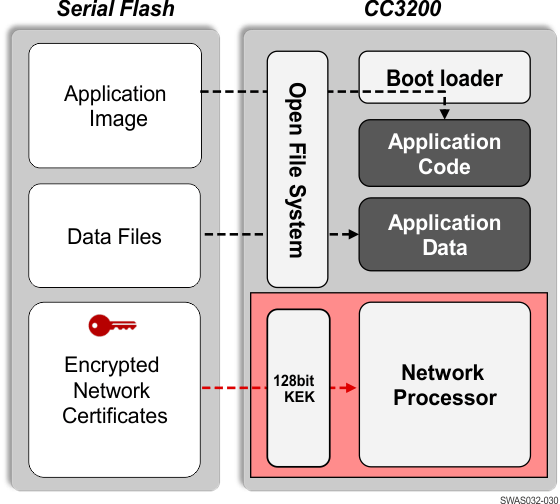 Figure 5-2 CC3200 Standard MCU
5.5 Wi-Fi Network Processor Subsystem
The Wi-Fi network processor subsystem includes a dedicated ARM MCU to completely offload the host MCU along with an 802.11 b/g/n radio, baseband, and MAC with a powerful crypto engine for a fast, secure WLAN and Internet connections with 256-bit encryption. The CC3200 device supports station, AP, and Wi-Fi Direct modes. The device also supports WPA2 personal and enterprise security and WPS 2.0. The Wi-Fi network processor includes an embedded IPv4 TCP/IP stack.
Table 5-1 summarizes the NWP features.
Table 5-1 Summary of Features Supported by the NWP Subsystem
| Item | Domain | Category | Feature | Details |
|---|---|---|---|---|
| 1 | TCP/IP | Network Stack | IPv4 | Baseline IPv4 stack |
| 2 | TCP/IP | Network Stack | TCP/UDP | Base protocols |
| 3 | TCP/IP | Protocols | DHCP | Client and server mode |
| 4 | TCP/IP | Protocols | ARP | Support ARP protocol |
| 5 | TCP/IP | Protocols | DNS/mDNS | DNS Address resolution and local server |
| 6 | TCP/IP | Protocols | IGMP | Up to IGMPv3 for multicast management |
| 7 | TCP/IP | Applications | mDNS | Support multicast DNS for service publishing over IP |
| 8 | TCP/IP | Applications | mDNS-SD | Service discovery protocol over IP in local network |
| 9 | TCP/IP | Applications | Web Sever/HTTP Server | URL static and dynamic response with template. |
| 10 | TCP/IP | Security | TLS/SSL | TLS v1.2 (client/server)/SSL v3.0 |
| 11 | TCP/IP | Security | TLS/SSL | For the supported Cipher Suite, go to SimpleLink Wi-Fi CC3200 SDK. |
| 12 | TCP/IP | Sockets | RAW Sockets | User-defined encapsulation at WLAN MAC/PHY or IP layers |
| 13 | WLAN | Connection | Policies | Allows management of connection and reconnection policy |
| 14 | WLAN | MAC | Promiscuous mode | Filter-based Promiscuous mode frame receiver |
| 15 | WLAN | Performance | Initialization time | From enable to first connection to open AP less than 50 ms |
| 16 | WLAN | Performance | Throughput | UDP = 16 Mbps |
| 17 | WLAN | Performance | Throughput | TCP = 12 Mbps |
| 18 | WLAN | Provisioning | WPS2 | Enrollee using push button or PIN method. |
| 19 | WLAN | Provisioning | AP Config | AP mode for initial product configuration (with configurable Web page and beacon Info element) |
| 20 | WLAN | Provisioning | SmartConfig | Alternate method for initial product configuration |
| 21 | WLAN | Role | Station | 802.11bgn Station with legacy 802.11 power save |
| 22 | WLAN | Role | Soft AP | 802.11 bg single station with legacy 802.11 power save |
| 23 | WLAN | Role | P2P | P2P operation as GO |
| 24 | WLAN | Role | P2P | P2P operation as CLIENT |
| 25 | WLAN | Security | STA-Personal | WPA2 personal security |
| 26 | WLAN | Security | STA-Enterprise | WPA2 enterprise security |
| 27 | WLAN | Security | STA-Enterprise | EAP-TLS |
| 28 | WLAN | Security | STA-Enterprise | EAP-PEAPv0/TLS |
| 29 | WLAN | Security | STA-Enterprise | EAP-PEAPv1/TLS |
| 30 | WLAN | Security | STA-Enterprise | EAP-PEAPv0/MSCHAPv2 |
| 31 | WLAN | Security | STA-Enterprise | EAP-PEAPv1/MSCHAPv2 |
| 32 | WLAN | Security | STA-Enterprise | EAP-TTLS/EAP-TLS |
| 33 | WLAN | Security | STA-Enterprise | EAP-TTLS/MSCHAPv2 |
| 34 | WLAN | Security | AP-Personal | WPA2 personal security |
5.6 Power-Management Subsystem
The CC3200 power-management subsystem contains DC-DC converters to accommodate the differing voltage or current requirements of the system.
- Digital DC-DC
- Input: VBAT wide voltage (2.1 to 3.6 V) or preregulated 1.85 V
- ANA1 DC-DC
- Input: VBAT wide voltage (2.1 to 3.6 V)
- In preregulated 1.85-V mode, the ANA1 DC-DC converter is bypassed.
- PA DC-DC
- Input: VBAT wide voltage (2.1 to 3.6 V)
- In preregulated 1.85-V mode, the PA DC-DC converter is bypassed.
In preregulated 1.85-V mode, the ANA1 DC-DC and PA DC-DC converters are bypassed. The CC3200 device is a single-chip WLAN radio solution used on an embedded system with a wide-voltage supply range. The internal power management, including DC-DC converters and LDOs, generates all of the voltages required for the device to operate from a wide variety of input sources. For maximum flexibility, the device can operate in the modes described in the following sections.
5.6.1 VBAT Wide-Voltage Connection
In the wide-voltage battery connection, the device is powered directly by the battery or preregulated 3.3-V supply. All other voltages required to operate the device are generated internally by the DC-DC converters. This scheme is the most common mode for the device as it supports wide-voltage operation from 2.1 to 3.6 V (for electrical connections, see Section 6.1.1, Typical Application – CC3200 Wide-Voltage Mode).
5.6.2 Preregulated 1.85 V
The preregulated 1.85-V mode of operation applies an external regulated 1.85 V directly at the pins 10, 25, 33, 36, 37, 39, 44, 48, and 54 of the device. The VBAT and the VIO are also connected to the 1.85-V supply. This mode provides the lowest BOM count version in which inductors used for PA DC-DC and ANA1 DC-DC (2.2 and 1 µH) and a capacitor (22 µF) can be avoided. For electrical connections, see Section 6.1.2, Typical Application – CC3200 Preregulated 1.85-V Mode.
In the preregulated 1.85-V mode, the regulator providing the 1.85 V must have the following characteristics:
- Load current capacity ≥900 mA.
- Line and load regulation with <2% ripple with 500 mA step current and settling time of <4 µs with the load step.
- The regulator must be placed very close to the CC3200 device so that the IR drop to the device is very low.
5.7 Low-Power Operating Mode
From a power-management perspective, the CC3200 device comprises the following two independent subsystems:
- Cortex-M4 application processor subsystem
- Networking subsystem
Each subsystem operates in one of several power states.
The Cortex-M4 application processor runs the user application loaded from an external serial flash. The networking subsystem runs preprogrammed TCP/IP and Wi-Fi data link layer functions.
The user program controls the power state of the application processor subsystem and can be in one of the five modes described in Table 5-2.
NOTE
Table 5-2 lists the modes by power consumption, with highest power modes listed first.
Table 5-2 User Program Modes
| Application Processor (MCU) Mode | Description |
|---|---|
| MCU active mode | MCU executing code at 80-MHz state rate |
| MCU sleep mode | The MCU clocks are gated off in sleep mode and the entire state of the device is retained. Sleep mode offers instant wakeup. The MCU can be configured to wake up by an internal fast timer or by activity from any GPIO line or peripheral. |
| MCU LPDS mode | State information is lost and only certain MCU-specific register configurations are retained. The MCU can wake up from external events or by using an internal timer. (The wake-up time is less than 3 ms.) Certain parts of memory can be retained while the MCU is in LPDS mode. The amount of memory retained is configurable. Users can choose to preserve code and the MCU-specific setting. The MCU can be configured to wake up using the RTC timer or by an external event on a GPIO (GPIO0–GPIO6). |
| MCU hibernate mode | The lowest power mode in which all digital logic is power-gated. Only a small section of the logic directly powered by the input supply is retained. The real-time clock (RTC) clock keeps running and the MCU supports wakeup from an external event or from an RTC timer expiry. Wake-up time is longer than LPDS mode at about 15 ms plus the time to load the application from serial flash, which varies according to code size. In this mode, the MCU can be configured to wake up using the RTC timer or external event on a GPIO (GPIO0–GPIO6). |
The NWP can be active or in LPDS mode and takes care of its own mode transitions. When there is no network activity, the NWP sleeps most of the time and wakes up only for beacon reception.
Table 5-3 Networking Subsystem Modes
| Network Processor Mode | Description |
|---|---|
| Network active mode processing layer 3, 2, and 1 | Transmitting or receiving IP protocol packets |
| Network active mode (processing layer 2 and 1) | Transmitting or receiving MAC management frames; IP processing not required. |
| Network active listen mode | Special power optimized active mode for receiving beacon frames (no other frames supported) |
| Network connected Idle | A composite mode that implements 802.11 infrastructure power save operation. The CC3200R network processor automatically goes into LPDS mode between beacons and then wakes to active listen mode to receive a beacon and determine if there is pending traffic at the access point. If not, the network processor returns to LPDS mode and the cycle repeats. |
| Network LPDS mode | Low-power state between beacons in which the state is retained by the network processor, allowing for a rapid wake up. |
| Network disabled |
The operation of the application and network processor ensures that the device remains in the lowest power mode most of the time to preserve battery life. Table 5-4 summarizes the important CC3200 chip-level power modes.
Table 5-4 Important Chip-Level Power Modes
| Power States for Applications MCU and Network Processor | Network Processor Active Mode (Transmit, Receive, or Listen) | Network Processor LPDS Mode | Network Processor Disabled |
|---|---|---|---|
| MCU active mode | Chip = active (C) | Chip = active | Chip = active |
| MCU LPDS mode | Chip = active (A) | Chip = LPDS (B) | Chip = LPDS |
| MCU hibernate mode | Not supported because chip is hibernated by MCU; thus, network processor cannot be in active mode | Not supported because chip is hibernated by MCU; thus, network processor cannot be in LPDS mode | Chip = hibernate (D) |
The following examples show the use of the power modes in applications:
- A product that is continuously connected to the network in the 802.11 infrastructure power-save mode but sends and receives little data spends most of the time in connected idle, which is a composite of modes A (receiving a beacon frame) and B (waiting for the next beacon).
- A product that is not continuously connected to the network but instead wakes up periodically (for example, every 10 minutes) to send data spends most of the time in mode D (hibernate), jumping briefly to mode C (active) to transmit data.
5.8 Memory
5.8.1 External Memory Requirements
The CC3200 device maintains a proprietary file system on the SFLASH. The CC3200 file system stores the service pack file, system files, configuration files, certificate files, web page files, and user files. By using a format command through the API, users can provide the total size allocated for the file system. The starting address of the file system cannot be set and is always located at the beginning of the SFLASH. The applications microcontroller must access the SFLASH memory area allocated to the file system directly through the CC3200 file system. The applications microcontroller must not access the SFLASH memory area directly.
The file system manages the allocation of SFLASH blocks for stored files according to download order, which means that the location of a specific file is not fixed in all systems. Files are stored on SFLASH using human-readable file names rather than file IDs. The file system API works using plain text, and file encryption and decryption is invisible to the user. Encrypted files can be accessed only through the file system (see Figure 5-2).
All file types can have a maximum of 128 supported files in the file system. All files are stored in blocks of 4KB and thus use a minimum of 4KB of flash space. Encrypted files with fail-safe support and optional security are twice the original size and use a minimum of 8KB. Encrypted files are counted as fail safe in terms of space. The maximum file size is 16MB.
Table 5-5 lists the SFLASH size recommendations.
Table 5-5 CC3200 SFLASH Size Recommendations
| Item | Typical Fail-Safe | Typical NonFail-Safe |
|---|---|---|
| File system | 20KB | 20KB |
| Service pack | 224KB | 112KB |
| System and configuration files | 216KB | 108KB |
| MCU code | 512KB | 256KB |
| Total | 4Mb | 2Mb |
| Recommended | 16Mb | 8Mb |
The CC3200 device supports JEDEC specification SFDP (serial flash device parameters). The following SFLASH devices are verified for functionality with the CC3200 device in addition to the ones in the reference design:
- Micron (N25Q128-A13BSE40): 128Mb
- Spansion (S25FL208K): 8Mb
- Winbond (W25Q16V): 16Mb
- Adesto (AT25DF081A): 8Mb
- Macronix (MX25L12835F-M2): 128Mb
For compatibility with the CC3200 device, the SFLASH device must support the following commands:
- Command 0x9F (read the device ID [JEDEC]). Procedure: SEND 0x9F, READ 3 bytes.
- Command 0x05 (read the status of the SFLASH). Procedure: SEND 0x05, READ 1 byte. Assume bit 0 is busy and bit 1 is write enable.
- Command 0x06 (set write enable). Procedure: SEND 0x06, read status until write-enable bit is set.
- Command 0xC7 (chip erase). Procedure: SEND 0xC7, read status until busy bit is cleared.
- Command 0x03 (read data). Procedure: SEND 0x03, SEND 24-bit address, read n bytes.
- Command 0x02 (write page). Procedure: SEND 0x02, SEND 24-bit address, write n bytes (0<n<256).
- Command 0x20 (sector erase). Procedure: SEND 0x20, SEND 24-bit address, read status until busy bit is cleared. Sector size is assumed to be always 4K.
5.8.2 Internal Memory
The CC3200 device includes on-chip SRAM to which application programs are downloaded and executed. The application developer must share the SRAM for code and data. To select the appropriate SRAM configuration, see the device variants listed in the orderable addendum at the end of this datasheet. The micro direct memory access (μDMA) controller can transfer data to and from SRAM and various peripherals. The CC3200 ROM holds the rich set of peripheral drivers, which saves SRAM space. For more information on drivers, see the CC3200 API list.
5.8.2.1 SRAM
The CC3200 family provides up to 256KB of zero-wait-state, on-chip SRAM. Internal RAM is capable of selective retention during LPDS mode. This internal SRAM is located at offset 0x2000 0000 of the device memory map.
Use the µDMA controller to transfer data to and from the SRAM.
When the device enters low-power mode, the application developer can choose to retain a section of memory based on need. Retaining the memory during low-power mode provides a faster wakeup. The application developer can choose the amount of memory to retain in multiples of 64KB. For more information, see the API guide.
5.8.2.2 ROM
The internal zero-wait-state ROM of the CC3200 device is at address 0x0000 0000 of the device memory and programmed with the following components:
- Bootloader
- Peripheral driver library (DriverLib) release for product-specific peripherals and interfaces
The bootloader is used as an initial program loader (when the serial flash memory is empty). The CC3200 DriverLib software library controls on-chip peripherals with a bootloader capability. The library performs peripheral initialization and control functions, with a choice of polled or interrupt-driven peripheral support. The DriverLib APIs in ROM can be called by applications to reduce flash memory requirements and free the flash memory to be used for other purposes.
5.8.2.3 Memory Map
Table 5-6 describes the various MCU peripherals and how they are mapped to the processor memory. For more information on peripherals, see the API document.
Table 5-6 Memory Map
| Start Address | End Address | Description | Comment |
|---|---|---|---|
| 0x0000 0000 | 0x0007 FFFF | On-chip ROM (Bootloader + DriverLib) | |
| 0x2000 0000 | 0x2003 FFFF | Bit-banded on-chip SRAM | |
| 0x2200 0000 | 0x23FF FFFF | Bit-band alias of 0x2000 0000 through 0x200F FFFF | |
| 0x4000 0000 | 0x4000 0FFF | Watchdog timer A0 | |
| 0x4000 4000 | 0x4000 4FFF | GPIO port A0 | |
| 0x4000 5000 | 0x4000 5FFF | GPIO port A1 | |
| 0x4000 6000 | 0x4000 6FFF | GPIO port A2 | |
| 0x4000 7000 | 0x4000 7FFF | GPIO port A3 | |
| 0x4000 C000 | 0x4000 CFFF | UART A0 | |
| 0x4000 D000 | 0x4000 DFFF | UART A1 | |
| 0x4002 0000 | 0x400 07FF | I2C A0 (Master) | |
| 0x4002 0800 | 0x4002 0FFF | I2C A0 (Slave) | |
| 0x4003 0000 | 0x4003 0FFF | General-purpose timer A0 | |
| 0x4003 1000 | 0x4003 1FFF | General-purpose timer A1 | |
| 0x4003 2000 | 0x4003 2FFF | General-purpose timer A2 | |
| 0x4003 3000 | 0x4003 3FFF | General-purpose timer A3 | |
| 0x400F 7000 | 0x400F 7FFF | Configuration registers | |
| 0x400F E000 | 0x400F EFFF | System control | |
| 0x400F F000 | 0x400F FFFF | µDMA | |
| 0x4200 0000 | 0x43FF FFFF | Bit band alias of 0x4000.0000 through 0x400F.FFFF | |
| 0x4401 C000 | 0x4401 EFFF | McASP | |
| 0x4402 0000 | 0x4402 0FFF | SSPI | Used for external serial flash |
| 0x4402 1000 | 0x4402 2FFF | GSPI | Used by application processor |
| 0x4402 5000 | 0x4402 5FFF | MCU reset clock manager | |
| 0x4402 6000 | 0x4402 6FFF | MCU configuration space | |
| 0x4402 D000 | 0x4402 DFFF | Global power, reset, and clock manager (GPRCM) | |
| 0x4402 E000 | 0x4402 EFFF | MCU shared configuration | |
| 0x4402 F000 | 0x4402 FFFF | Hibernate configuration | |
| 0x4403 0000 | 0x4403 FFFF | Crypto range (includes apertures for all crypto-related blocks as follows) | |
| 0x4403 0000 | 0x4403 0FFF | DTHE registers and TCP checksum | |
| 0x4403 5000 | 0x4403 5FFF | MD5/SHA | |
| 0x4403 7000 | 0x4403 7FFF | AES | |
| 0x4403 9000 | 0x4403 9FFF | DES | |
| 0xE000 0000 | 0xE000 0FFF | Instrumentation trace Macrocell™ | |
| 0xE000 1000 | 0xE000 1FFF | Data watchpoint and trace (DWT) | |
| 0xE000 2000 | 0xE000 2FFF | Flash patch and breakpoint (FPB) | |
| 0xE000 E000 | 0xE000 EFFF | Nested vectored interrupt controller (NVIC) | |
| 0xE004 0000 | 0xE004 0FFF | Trace port interface unit (TPIU) | |
| 0xE004 1000 | 0xE004 1FFF | Reserved for embedded trace macrocell (ETM) | |
| 0xE004 2000 | 0xE00F FFFF | Reserved |
5.9 Boot Modes
5.9.1 Overview
The boot process of the application processor includes two phases. The first phase consists of unrestricted access to all register space and configuration of the specific device setting. In the second phase, the application processor executes user-specific code.
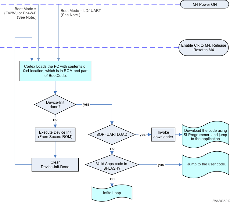
Figure 5-3 shows the bootloader flow chart.
5.9.2 Invocation Sequence/Boot Mode Selection
The following sequence of events occur during the Cortex processor boot:
- After power-on-reset (POR), the processor starts execution.
- The processor jumps to the first few lines (FFL) of code in the ROM to determine if the current boot is the first device-init boot or the second MCU boot. The determination is based on the Device-Init flag in a secure register. The Device-Init flag is set out of POR. The registers in the secure region are accessible only in the device-init mode.
- If the current boot is the first boot, the processor executes the device-init code from ROM.
- At the end of the boot, the processor clears the Device-Init flag and changes the master ID of the processor and the DMA. These registers are part of the secure region.
- The processor resets itself, initiating a second boot.
- During the second boot, the processor rereads the Device-Init flag, the bit is cleared, and the processor obtains a different master ID.
- After executing FFL and the unsecure boot code, the processor jumps to the developer code (application).
- For the rest of the operation (until the next power cycle), the Cortex mode is designated the MCU. During this phase, access to the secure region is restricted.
5.9.3 Boot Mode List
The CC3200 device implements a sense-on-power (SoP) scheme to determine the device operation mode. The device can be configured to power up in one of the three following modes:
- Fn4WJ: Functional mode with a 4-wire JTAG mapped to fixed pins.
- Fn2WJ: Functional mode with a 2-wire SWD mapped to fixed pins.
- LDfrUART: UART load mode to flash the system during development and in OEM assembly line (for example, serial flash connected to the CC3200R device).
SoP values are sensed from the device pin during power up. This encoding determines the boot flow. Before the device is taken out of reset, the SoP values are copied to a register and then determine the device opeartion mode while powering up. These values determine the boot flow as well as the default mapping for some of the pins (JTAG, SWD, UART0) Table 5-7 show the pull configurations.
Table 5-7 CC32x0 Functional Configurations
| Name | SoP[2] | SoP[1] | SoP[0] | SoP Mode | Comment |
|---|---|---|---|---|---|
| UARTLOAD | Pullup | Pulldown | Pulldown | LDfrUART | Factory/Lab Flash/SRAM load through UART. Device waits indefinitely for UART to load code. The SOP bits then must be toggled to configure the device in functional mode. Also puts JTAG in 4-wire mode. |
| FUNCTIONAL_2WJ | Pulldown | Pulldown | Pullup | Fn2WJ | Functional development mode. In this mode, two-pin SWD is available to the developer. TMS and TCK are available for debugger connection. |
| FUNCTIONAL_4WJ | Pulldown | Pulldown | Pulldown | Fn4WJ | Functional development mode. In this mode, four-pin JTAG is available to the developer. TDI, TMS, TCK, and TDO are available for debugger connection. |
The recommended value of pull resistors for SOP0 and SOP1 is 100 kΩ and 2.7 kΩ for SOP2. SOP2 can be used by the application for other functions after chip power-up is complete. However, to avoid spurious SOP values from being sensed at power-up, TI strongly recommends that the SOP2 pin be used only for output signals. On the other hand, the SOP0 and SOP1 pins are multiplexed with WLAN analog test pins and are not available for other functions.